
Electrophotographic photoconductor, and image forming process, image forming apparatus and process cartridge for an image forming apparatus using the same

a photoconductor and electrochemical technology, applied in the field of electrochemical photocondu, can solve the problems of sensitivity and chargeability, deterioration of electrical properties, and abrasion resistance, and achieve excellent properties, high elasticity, and high abrasion resistance

Active Publication Date: 2007-02-13
RICOH KK
View PDF17 Cites 50 Cited by
  • Summary
  • Abstract
  • Description
  • Claims
  • Application Information

AI Technical Summary

Benefits of technology

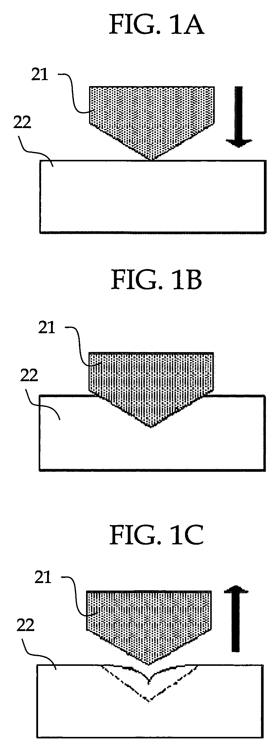
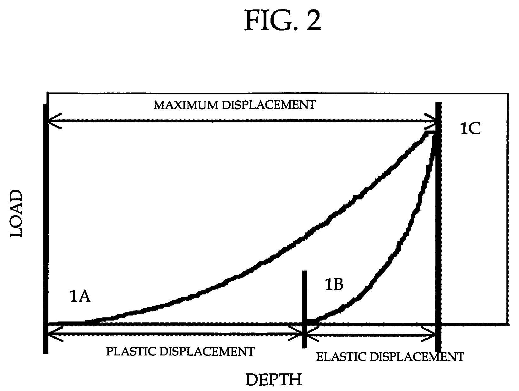
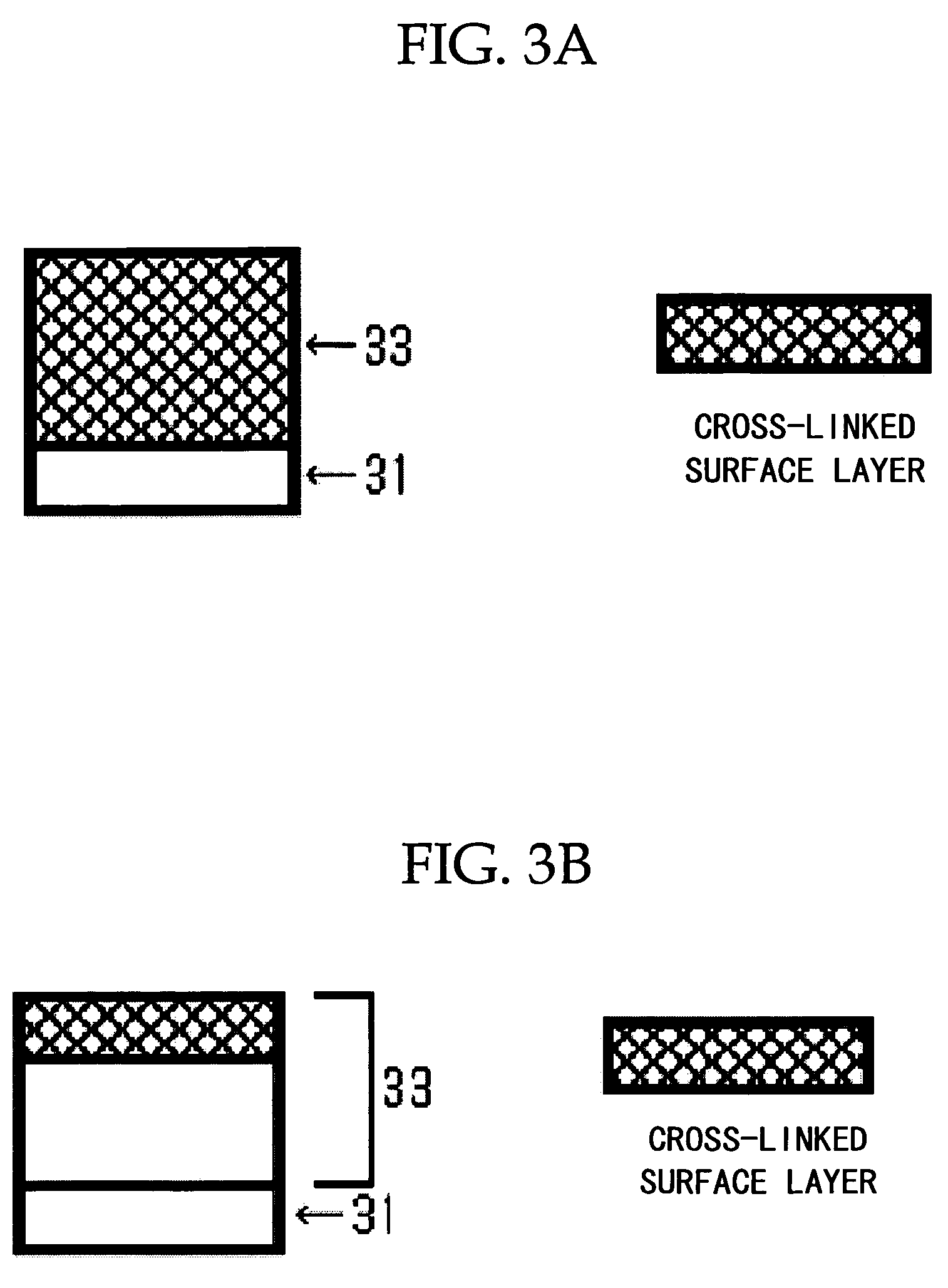
The present invention provides an electrophotographic photoconductor with a cross-linked surface layer that has high abrasion resistance and excellent properties, such as elasticity and uniform surface layer. This photoconductor can prevent image deterioration and plastic deformation, resulting in long-lasting, high-quality images. The invention also provides an image forming process, image forming apparatus, and process cartridge for the image forming apparatus using this electrophotographic photoconductor. The cross-linked surface layer of the photoconductor has an elastic displacement rate of τe of 35% or more and a standard deviation of τe of 2% or less. The mono-functional radical polymerizable monomer used in the cross-linked surface layer has a functional group of acryloyloxy group or methacryloyloxy group. The mono-functional radical polymerizable compound used in the cross-linked surface layer has a charge transporting structure of triarylamine structure or a triarylene group. The invention also provides a photoconductor with improved elasticity and uniform cross-linked surface layer formed by curing at least a tri- or more-functional radical polymerizable monomer without having a charge transporting structure. The mono-functional radical polymerizable compound used in the cross-linked surface layer has a ratio of molecular weight to number of functional group of 250 or less. The invention also provides a photoconductor with improved abrasion resistance and durability. The invention also provides an image forming process and apparatus using this electrophotographic photoconductor.

Problems solved by technology

In this point of view, the organic photoconductor has a defect in that when it is repeatedly used in the electrophotographic process, it is susceptible to abrasion by mechanical load of a developing system or a cleaning system since the surface layer comprises mainly a low molecular charge transport material and an inactive high molecule (polymer) which are generally soft.
Such abrasion of the photoconductor leads deterioration of electrical properties such as sensitivity and chargeability and thereby, deteriorated image with reduction of image density and contamination of the ground surface.
Also, a damaged part with local abrasion produces a contaminated image with a striped pattern by cleaning failure.
Among these techniques, the use of a curable binder in (1) tends to cause reduction in image density since the curable binder has poor compatibility with the charge transporting material and impurities such as a polymerization initiator and unreacted residue increases residual potential.
However, it is not sufficient for satisfying the durability required in the organic photoconductor.
Further, it is difficult to polymerize and purify the high molecular (polymer) charge transporting material.
Thus, it is impossible to obtain it at a high purity and to attain stable electrical properties between materials upon using it.
In addition, it may cause problems such as high viscosity of the coating solution in terms of the preparation.
However, traps on the surface of the inorganic filler tends to increase the residual potential, thereby causing reduction in the image density.
Also, when unevenness of the inorganic filler and the binder resin on the surface of the photoconductor is severe, cleaning failure may occur, resulting in toner peeling and image deletion.
With these techniques of (1), (2) and (3), it is impossible to satisfy the durability required for the organic photoconductor, including electrical durability and mechanical durability.
The photoconductor used in this technique may inhibit increase of residual potential by repeated use.
However, it has defects in that since resistance of the protective layer decreases in a high humidity circumstance, reduction of resolution and image deletion may occur.
Further, when a low molecular charge transport material is simply added to the surface layer, it may cause problems related with the compatibility to the cured body, whereby crystallization of the low molecular charge transporting material and clouding may occur, resulting in reduction in mechanical properties.
In addition, according to this photoconductor, since the monomer is reacted while it contains a high molecular binder, the curing cannot be sufficiently progressed.
Also, the cured body is poorly compatible with the binder resin and surface unevenness by phase separation upon curing may occur, causing cleaning failure.
However, when a non-reactive resin is used as the binder resin, the binder resin is poorly compatible with the cured body produced by the reaction of the monomer and the charge transport material, whereby surface unevenness during cross-linking forms from the phase separation, resulting in cleaning failure.
Also, as described above, in addition to the interference of the binder resin with the curing of the monomer, a bi-functional monomer which can be used in the photoconductor has a few functionality and fails to provide a sufficient cross-linkage density, whereby it is possible to obtain a sufficient abrasion resistance.
Also, when a reactive binder is used, since the number of functional groups contained in the monomer and the binder resin is small, the bonding of the charge transporting material and the cross-linkage density cannot be satisfied at the same time and the electrical properties and abrasion resistance are not sufficient.
However, according to the photoconductive layer, since a big hole transporting compound has two or more chain polymerizable functional group, distortion may occur in a cured body, causing increase in internal stress, roughness of the surface layer and formation of crack over the time.
Even in a photoconductor having a cross-linked photoconductive layer with a charge transporting structure chemically attached, it cannot be said that general properties are sufficiently attained.

Method used


Image

  • Electrophotographic photoconductor, and image forming process, image forming apparatus and process cartridge for an image forming apparatus using the same
  • Electrophotographic photoconductor, and image forming process, image forming apparatus and process cartridge for an image forming apparatus using the same
  • Electrophotographic photoconductor, and image forming process, image forming apparatus and process cartridge for an image forming apparatus using the same

Examples


example

[0244]Now, the present invention will be explained in further detail by the following Example s. However, the present invention is not limited thereto. Also, all parts in the text are by weight.

example a-1

[0245]On a φ30 mm aluminum cylinder, a coating solution for a under coating layer, a coating solution for a charge generation layer, a coating solution for a charge transport layer, each coating solution has a composition described below, were sequentially applied and dried to form a under coating layer of 3.5 μm, a charge generation layer of 0.2 μm and a charge transport layer of 18 μm. On the charge transport layer, a coating solution for a surface crosslinked layer of a composition described below was spray coated, irradiated under conditions of a metal halide lamp: 160 W / cm, irradiation distance: 120 mm, irradiation intensity: 500 mW / cm2, irradiation time: 20 seconds, and further dried at 130° C. for 20 to prepare a surface cross-linked layer of 4 μm. Thus, an electrophotographic photoconductor according to the present invention is formed.

[Coating Solution for a Under Coating Layer]

[0246]

Alkyde resin 6 parts(Bekozole 1307-60-EL, DAINIPPON INK AND CHEMICALS,INCORPORATED)Melamine ...

example a-2

[0250]An electrophotographic photoconductor was prepared following the procedures in Example A-1 except that the tri- or more-functional radical polymerizable monomer without having a charge transporting structure contained in the coating solution for a surface crosslinked layer of Example A-1 was substituted with the following monomer.

[0251]

Tri- or more-functional radical polymerizable monomer10 partswithout having a charge transporting structureDitrimethylolpropane tetraacrylate (SR-355, SartomerCompany Inc.)Molecular weight: 466, number of functional group: 4functionality, molecular weight / number of functionalgroup = 117


PUM


Abstract

Disclosed is an electrophotographic photoconductor including at least a photoconductive layer on a conductive substrate, wherein the surface layer of the photoconductive layer contains at least a surface crosslinked layer formed by curing a tri- or more-functional radical polymerizable monomer without having a charge transporting structure and a mono-functional radical polymerizable compound having a charge transporting structure and the surface crosslinked layer has a surface roughness Rz of 1.3 μm or less.

Description

BACKGROUND OF THE INVENTION[0001]1. Field of the Invention[0002]The present invention relates to an electrophotographic photoconductor with high durability which is capable of realizing high quality of images for a long period of time. Also, it relates to an image forming process, an image forming apparatus and a process cartridge for an image forming apparatus using the long life and high performance photoconductor.[0003]2. Description of the Related Art[0004]Recently, the organic photoconductor (OPC) is widely used in a copying machine, facsimile, laser printer and a composite thereof owing to excellent performance and various advantages, instead of the inorganic photoconductor. The reason includes, for example, (1) optical properties such as range of light absorbing wave length and absorption amount, (2) electrical properties such as high sensitivity, stable charging properties, (3) width of selection range of materials, (4) easiness of preparation, (5) low cost, (6) non-toxicity...

Claims


Application Information

Patent Timeline
Patent Type & Authority Patents(United States)
IPC IPC(8): G03G5/147G03G5/047G03G5/05
CPCG03G5/047G03G5/0592G03G5/05
Inventor SUZUKI, TETSUROTAMURA, HIROSHIIKUNO, HIROSHINAGAI, KAZUKIYOLI, HONGGUO
Owner RICOH KK
Learn More