
Fabrication process of semiconductor package and semiconductor package

a technology of semiconductor packaging and semiconductor packaging, which is applied in the manufacture of printed circuits, basic electric elements, printed circuit assembling, etc., can solve the problems of warping in the package due to a difference in thermal stress between the mother board and the package, and the type of printed wiring boards is also accompanied by, so as to reduce the effect of strain elimination, lessen the relaxation effect, and eliminate the residual strain

Inactive Publication Date: 2007-03-06
HITACHI CHEM CO LTD
View PDF64 Cites 57 Cited by
  • Summary
  • Abstract
  • Description
  • Claims
  • Application Information

AI Technical Summary

Benefits of technology

[0056]The predetermined number of wiring per unit in step 6B is preferred to be one. However, in order to improve productivity, it can be more than one.
[0095]The heat treatment can be conducted preferably at a temperature in a range of the glass transition point of the hardened sealing resin ±20° C., because the hardened resin exhibits strongest plastic properties in the range of the glass transition point of the hardened sealing resin ±20° C., thereby facilitating elimination of residual strain. If the temperature of the heat treatment is lower than the glass transition point −20° C., the hardened resin becomes a glassy elastic substance so that relaxation effects tend to be lessened. If the temperature is higher than the glass transition point +20° C., the hardened resin turns to a rubbery elastic substance so that effect of strain elimination also tend to be reduced.
[0096]A warp or deformation in the semiconductor package can be more completely eliminated by cooling the semiconductor package to room temperature at a temperature-lowering rate of 5° C. / min or less after the semiconductor package is heat-treated at a temperature in the temperature of the glass transition point of the hardened sealing resin ±20° C.
[0097]It is preferred to conduct the heat-treatment and / or cooling step while pressing upper and lower surfaces of the hardened sealing resin by rigid flat plates under forces that reduce a warp or deformation in the hardened sealing resin.

Problems solved by technology

However, their connections with printed boards are conducted by insertion, so that they are not suited for surface mounting.
Of these, the ceramic type has a shorter distance between a mother board and a package compared with the conventional PGAs so that a warp in the package due to a difference in thermal stress between the mother board and the package remains a serious problem.
Further, the printed wiring board type is also accompanied by problems such as substrate warping, low moisture resistance, low reliability and large substrate thickness.
In contrast, upon forming a two-layer flexible base material into the form of a leadframe and handling the same, a base film of a small thickness involves problems such as low handling readiness and insufficient rigidity as a frame.

Method used


Image

  • Fabrication process of semiconductor package and semiconductor package
  • Fabrication process of semiconductor package and semiconductor package
  • Fabrication process of semiconductor package and semiconductor package

Examples


specific example 1

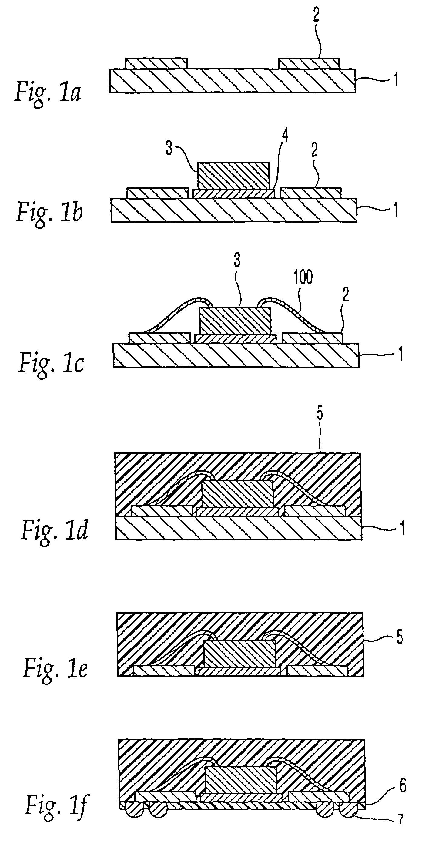
[0162]A two-layer flexible base material having an electrolytic copper foil of 12 μm in thickness on one side thereof (“MCF 50001”, trade name; product of Hitachi Chemical Co., Ltd.) was provided. A dry film resist (“PHOTEC HK815”, trade name; product of Hitachi Chemical Co., Ltd.) was laminated on the copper foil and then exposed and developed, whereby a desired resist pattern was obtained. After the copper foil was etched with a solution of ferric chloride, the resist pattern was stripped with a solution of potassium hydroxide so that a predetermined wiring pattern was obtained. Using an excimer laser beam machine (“INDEX 200”, trade name; manufactured by Sumitomo Heavy Industries, Ltd.), as many holes as needed (diameter: 300 μm) were formed at predetermined positions so that they extend from a side of an insulating base material and reach a back surface of the wiring pattern. The following conditions were set for the excimer laser beam machiningenergy density: 250 mJ / cm2, reduc...

specific example 2

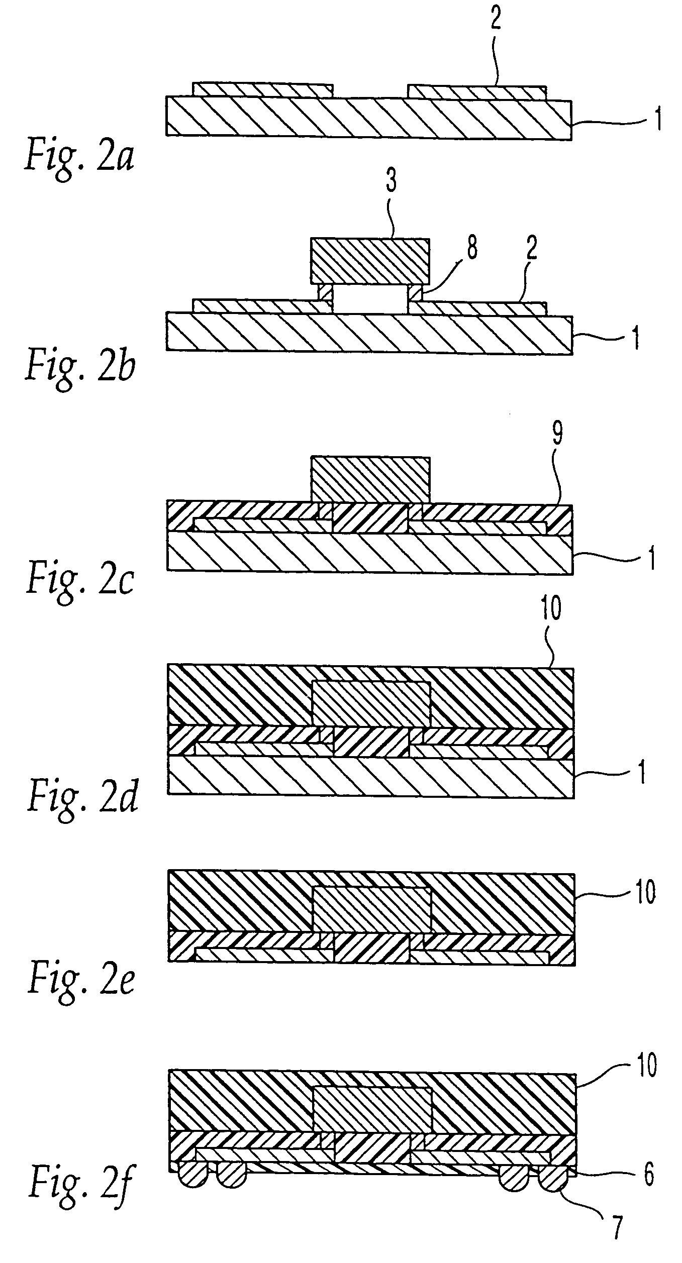
[0168]A two-layer flexible base material having an electrolytic copper foil of 12 μm in thickness on one side thereof (“MCF 50001”, trade name; product of Hitachi Chemical Co., Ltd.) was provided. A dry film resist (“PHOTEC HK815”, trade name; product of Hitachi Chemical Co., Ltd.) was laminated on the copper foil and then exposed and developed, whereby a desired resist pattern was obtained. After the copper foil was etched with a solution of ferric chloride, the resist pattern was stripped with a solution of potassium hydroxide so that a predetermined wiring pattern was obtained. Using an excimer laser beam machine (“INDEX 200”, trade name; manufactured by Sumitomo Heavy Industries, Ltd.), as many holes as needed (diameter: 300 μm) were formed as many as needed at predetermined positions so that they extend from a side of an insulating base material and reach a back surface of the wiring pattern. The following conditions were set for the excimer laser beam machiningenergy density:...

specific example 3

[0174]On a shiny surface of an electrolytic copper foil of 35 μm in thickness and 250 mm squares in external shape, a photosensitive dry film resist (“PHOTEC HN640”, trade name; product of Hitachi Chemical Co., Ltd.) was laminated, followed by exposure and development so that a desired resist pattern (minimum line / space=50 μm / 50 μm) was formed. As many as 300 (4 blocks / 250 mm squares, 75 patterns / block) identical wiring patterns which were each consisted of 0.2 μm thick nickel, 30 μm thick copper, 5 μm thick nickel and 1 μm thick soft gold were next formed by an electroplating method. The resist pattern was next stripped off using a 3 wt. % solution of potassium hydroxide of 35° C. The resultant assembly was dried at 85° C. for 15 minutes and then cut into the individual blocks. Using a semiconductor-device-mounting die-bonding material (“HM-1”, trade name; product of Hitachi Chemical Co., Ltd.), semiconductor devices were then bonded. The bonding conditions were set as follows—pres...


PUM


Abstract

A semiconductor package substrate is provided, which can meet the move toward high integration of semiconductors. A nickel layer is plated on an electroplated copper foil to form a wiring pattern. An LSI chip is mounted on the copper foil, and terminals of the LSI chip and the wiring pattern are connected by wire bonding, followed by sealing with a semiconductor-sealing epoxy resin. Only the copper foil is dissolved away with an alkali etchant to expose nickel. With a nickel stripper having low copper-dissolving power, the nickel layer is removed to expose the wiring pattern. A solder resist is coated, and a pattern is formed in such a way that connecting terminal portions are exposed. Solder balls are placed at the exposed portions of the wiring pattern and are then fused. The wiring pattern is connected to an external printed board via the solder balls.

Description

[0001]This application is a division of U.S. application Ser. No. 10 / 008,616, filed on Oct. 23, 2001 now U.S. Pat. No. 6,746,897, which is a continuation of U.S. application Ser. No. 09 / 487,682, filed on Jan. 19, 2000 now U.S. Pat. No. 6,365,432, which is a division of U.S. application Ser. No. 09 / 326,316, filed on Jun. 7, 1999, now abandoned, which is a continuation of U.S. application Ser. No. 08 / 716,362, filed on Sep. 18, 1996, now U.S. Pat. No. 5,976,912.TECHNICAL FIELD[0002]This invention relates to a process for the fabrication of a semiconductor package and also to a semiconductor package.BACKGROUND ART[0003]As the level of integration of semiconductors becomes higher, the number of input / output terminals increases. A need has therefore arisen for a semiconductor package having many input / output terminals. In general, input / output terminals can be divided into two types, one being those arranged in a single row along a periphery of a package and the other being those arranged...

Claims


Application Information

Patent Timeline
IPC IPC(8): H01L21/00H01L21/48H01L21/56H01L21/58H01L21/68H01L23/31H01L23/498H05K3/20
CPCH01L21/4803H01L21/56H01L21/561H01L21/568H01L23/3121H01L23/3128H01L23/49811H01L23/49816H01L23/4985H01L24/32H01L24/83H01L24/97H01L2221/68377H01L2224/16237H01L2224/32057H01L2224/32225H01L2224/48091H01L2224/48227H01L2224/48228H01L2224/73204H01L2224/73265H01L2224/83001H01L2224/83102H01L2224/8319H01L2224/83385H01L2224/8385H01L2224/85001H01L2224/92125H01L2224/97H01L2924/01004H01L2924/01005H01L2924/01015H01L2924/01027H01L2924/01029H01L2924/01033H01L2924/01047H01L2924/0105H01L2924/01078H01L2924/01079H01L2924/01082H01L2924/01322H01L2924/01327H01L2924/07802H01L2924/14H01L2924/15153H01L2924/1517H01L2924/15184H01L2924/15311H05K3/20H01L2924/01006H01L2924/014H01L24/48H01L2224/2919H01L2924/01019H01L2924/0665H01L2224/45144H01L2224/32245H01L2224/48247H01L2924/07811H01L2224/32503H01L2224/8381H01L2224/85H01L2924/00014H01L2224/83H01L2224/92247H01L2924/00H01L2924/00012H01L2924/351H01L2924/203H01L2924/12042H01L24/45H01L2924/181H01L24/73H01L2924/15183H01L2224/29339H01L2924/00015H01L2924/0002H01L2224/16225H01L23/12H05K3/30
Inventor FUKUTOMI, NAOKITSUBOMATSU, YOSHIAKIINOUE, FUMIOYAMAZAKI, TOSHIOOHHATA, HIROHITOHAGIWARA, SHINSUKETAGUCHI, NORIYUKINOMURA, HIROSHI
Owner HITACHI CHEM CO LTD
Learn More