Semiconductor device having SiGe channel region

a technology of sige channel and semiconductor, which is applied in the direction of semiconductor devices, electrical devices, transistors, etc., can solve the problems of low threshold voltage, significant increase of body resistance, and the necessity of reducing the threshold voltage, so as to achieve low threshold voltage and wide operation range. , the effect of high speed

Inactive Publication Date: 2007-04-17
PANNOVA SEMIC
View PDF10 Cites 94 Cited by
  • Summary
  • Abstract
  • Description
  • Claims
  • Application Information

AI Technical Summary

Benefits of technology

[0012]It is an object of the present invention to provide a semiconductor device functioning as ...

Problems solved by technology

In this case, however, the leakage current at the time when the gate is off becomes large, so that it is inevitable that there should be a lower limit for threshold voltage.
Furthermore, in the conventional DTMOS, the necessity of reducing the threshold voltage does not allow the impurity concentration of the body to be high.
As a result, the resistance of the body becomes significantly high, so that the voltage drop at the body prevents efficient conduction of the electric potential of the gate...

Method used


Image

  • Semiconductor device having SiGe channel region
  • Semiconductor device having SiGe channel region
  • Semiconductor device having SiGe channel region

Examples


first embodiment

[0079]In this embodiment, examples of DTMOS utilizing a Si / SiGe heterojunction using SiGe as a material constituting a channel region.

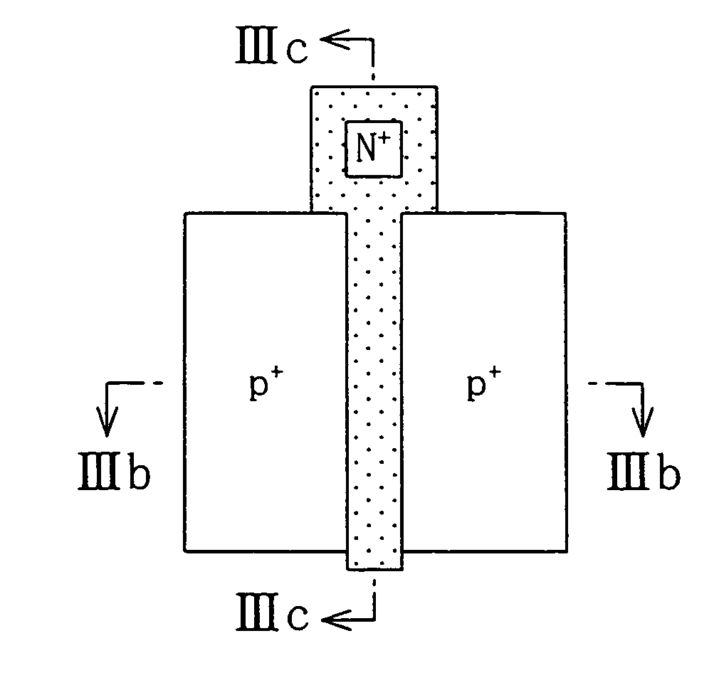
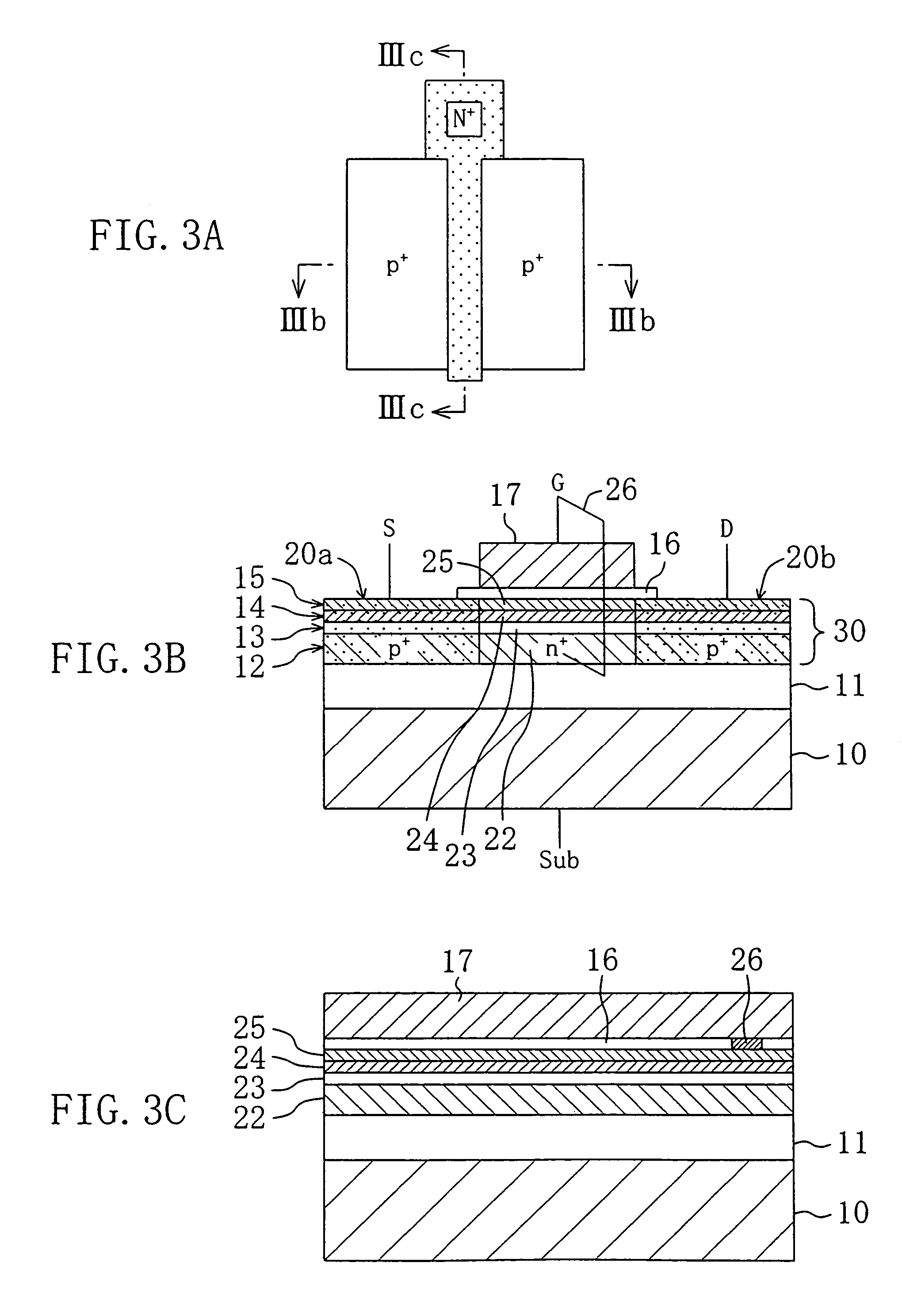
[0080]FIG. 3A is a plan view schematically showing the structure of a HDTMOS of this Embodiment. FIG. 3B is a cross-sectional view taken along line IIIb—IIIb of FIG. 3A. FIG. 3C is a cross-sectional view taken along line IIIc—IIIc of FIG. 3A. As shown in FIGS. 3A to 3C, the HDTMOS of this embodiment includes a p-type Si substrate 10, a buried oxide film 11 formed on the Si substrate, for example by a method of implanting oxygen ions, and a semiconductor layer 30 provided on the buried oxide film 11. The semiconductor layer 30 includes an upper Si film 12 constituting an upper portion of the SOI substrate, a Si buffer layer 13 epitaxially grown by a UHV-CVD method on the upper Si film 12, a SiGe film 14 epitaxially grown by a UHV-CVD method on the Si buffer layer 13, and a Si film 15 epitaxially grown by a UHV-CVD method on the SiGe film 14. Furthermor...

second embodiment

[0112]In this embodiment, an example of an n-channel HDTMOS using SiGe as a material constituting the channel region will be described.

[0113]FIG. 17A is a plan view schematically showing the structure of a HDTMOS of this embodiment. FIG. 17B is a cross-sectional view taken along line XVIIb—XVIIb of FIG. 17A. FIG. 17C is a cross-sectional view taken along line XVIIc—XVIIc of FIG. 17A. As shown in FIGS. 17A to 17C, the HDTMOS of this embodiment includes a p-type Si substrate 50, a buried oxide film 51 formed by a method, for example, of implanting oxygen ions to the Si substrate, and a semiconductor layer 80 formed on the buried oxide film 51. The semiconductor layer 80 includes an upper Si film 52 constituting the upper portion of the SOI substrate, a Si buffer layer 53 epitaxially grown by a UHV-CVD method on the upper Si film 52, a SiGe film 54 epitaxially grown by a UIIV-CVD method on the Si buffer layer 53, and a Si film 55 epitaxially grown by a UHV-CVD method on the SiGe film 5...

third embodiment

[0119]In this embodiment, an example of a complementary HDTMOS using SiGe as a material constituting the channel region will be described.

[0120]FIG. 22 is a cross-sectional view showing the structure of a complementary HDTMOS of this embodiment. As shown in FIG. 22, the HDTMOS of this embodiment includes a p-type Si substrate 10, a buried oxide film 11 formed by a method, for example, of implanting oxygen ions to the Si substrate, a semiconductor layer 30 for a p-channel type HDTMOS (p-DTMOS) formed on the buried oxide film 11, and a semiconductor layer 80 for an n-channel type HDTMOS (n-DTMOS) formed on the buried oxide film 11. The semiconductor layers 30 and 80 include the films described in the first and second embodiments. The HDTMOS includes gate insulator films 16 and 56 made of a silicon oxide film formed on the semiconductor layers 30 and 80, respectively, gate electrode 17 and 57 formed on the gate insulator films 16 and 56, respectively, and side walls 18 and 58 provided ...


PUM


Abstract

A HDTMOS includes a Si substrate, a buried oxide film and a semiconductor layer. The semiconductor layer includes an upper Si film, an epitaxially grown Si buffer layer, an epitaxially grown SiGe film, and an epitaxially grown Si film. Furthermore, the HDTMOS includes an n-type high concentration Si body region, an nSi region, a SiGe channel region containing n-type low concentration impurities, an n-type low concentration Si cap layer, and a contact which is a conductor member for electrically connecting the gate electrode and the Si body region. The present invention extends the operation range while keeping the threshold voltage small by using, for the channel layer, a material having a smaller potential at the band edge where carriers travel than that of a material constituting the body region.

Description

[0001]This application is a continuation of application Ser. No. 10 / 268,905 filed Oct. 11, 2002, which is a continuation of application Ser. No. 09 / 712.223, filed Nov. 15, 2000, now U.S. Pat. No. 6,512,252.BACKGROUND OF THE INVENTION[0002]The present invention relates to a semiconductor device that functions as a DTMOS or a MISFET having a heterojunction active region.[0003]In recent years, portable information terminal units driven by a battery are widely used. In such units, there is a strong demand for reducing the power supply voltage without compromising high speed operations in order to prolong the battery lifetime. Reducing the threshold voltage is effective in realizing high speed operations. In this case, however, the leakage current at the time when the gate is off becomes large, so that it is inevitable that there should be a lower limit for threshold voltage.[0004]As a device that can solve this problem and has a small leakage current at a low voltage and high driving ab...

Claims


Application Information

Patent Timeline
IPC IPC(8): H01L31/072H01L21/84H01L29/161H01L29/165H01L29/778H01L29/786
CPCH01L21/84H01L27/1203H01L29/1054H01L29/7782H01L29/783H01L29/78615H01L29/78648H01L29/78687H01L29/161H01L29/165
Inventor TAKAGI, TAKESHIINOUE, AKIRA
Owner PANNOVA SEMIC
Why Eureka
Try Eureka