Ultra scalable high speed heterojunction vertical n-channel MISFETs and methods thereof

a heterojunction, n-channel technology, applied in the field of metal insulator semiconductor field effect transistors, can solve the problems of difficult to achieve abrupt doping profiles, traditional techniques fail to reduce certain undesirable physical effects, and the scaling of silicon mosfets has become a major challenge, so as to achieve superb performance and scalability, optimize drive current and leakage current, and avoid tradeoffs in conventional si technology.

Active Publication Date: 2007-04-17
GLOBALFOUNDRIES US INC
View PDF12 Cites 98 Cited by
  • Summary
  • Abstract
  • Description
  • Claims
  • Application Information

AI Technical Summary

Benefits of technology

[0013]The objective of this invention is to provide a device structure that has superb performance and scalability. By using 2-dimensional bandgap engineering, the tradeoffs in the conventional Si technology can be avoided, and the drive current and leakage current can be optimized independently. Consequently, very high drive current and excellent turn-off characteristics can be achieved simultaneously. Moreover, the suppression of short-channel effects in such a device further allows continuous and more aggressive scaling of the MOSFET technology.

Problems solved by technology

Silicon MOSFET scaling has become a major challenge in the semiconductor industry.
Traditional techniques start to fail in reducing certain undesirable physical effects as device dimensions shrink down to the nanometer regime.
However, the abrupt doping profiles are difficult to achieve due to temperature enhanced diffusion, and these highly doped channels or pocket implant regions increase junction capacitance and band-to-band tunneling.
It has been shown by S. Thompson, et al., in “MOS scaling: transistor challenges for the 21st century,” Intel Technology Journal, Q3, 1998, that channel engineering can only decrease the circuit gate delay by ˜10% for a given technology, and it cannot provide channel length scaling for generation after generation that gate oxide and source / drain (S / D) junction depth scaling has provided.
However, two prominent problems still remain in these planar devices: device scaling and control of short-channel effects.
However, SOI does not remove short-channel effects completely, and an inherent problem with SOI is the floating body effect.
Even though very short channels may be achieved and short-channel effects may be reduced, there is still a big drawback with such device structures.
However, at the on state (i.e., high bias at the gate and drain), the built-in hetero-barrier becomes harmful to the drive current.
This is because the hetero-barrier at the source / channel junction severely blocks the thermal emission of the carriers from the source into the channel.
However, it is a planar structure and still suffers from the short-channel effects.

Method used


Image

  • Ultra scalable high speed heterojunction vertical n-channel MISFETs and methods thereof
  • Ultra scalable high speed heterojunction vertical n-channel MISFETs and methods thereof
  • Ultra scalable high speed heterojunction vertical n-channel MISFETs and methods thereof

Examples


first embodiment

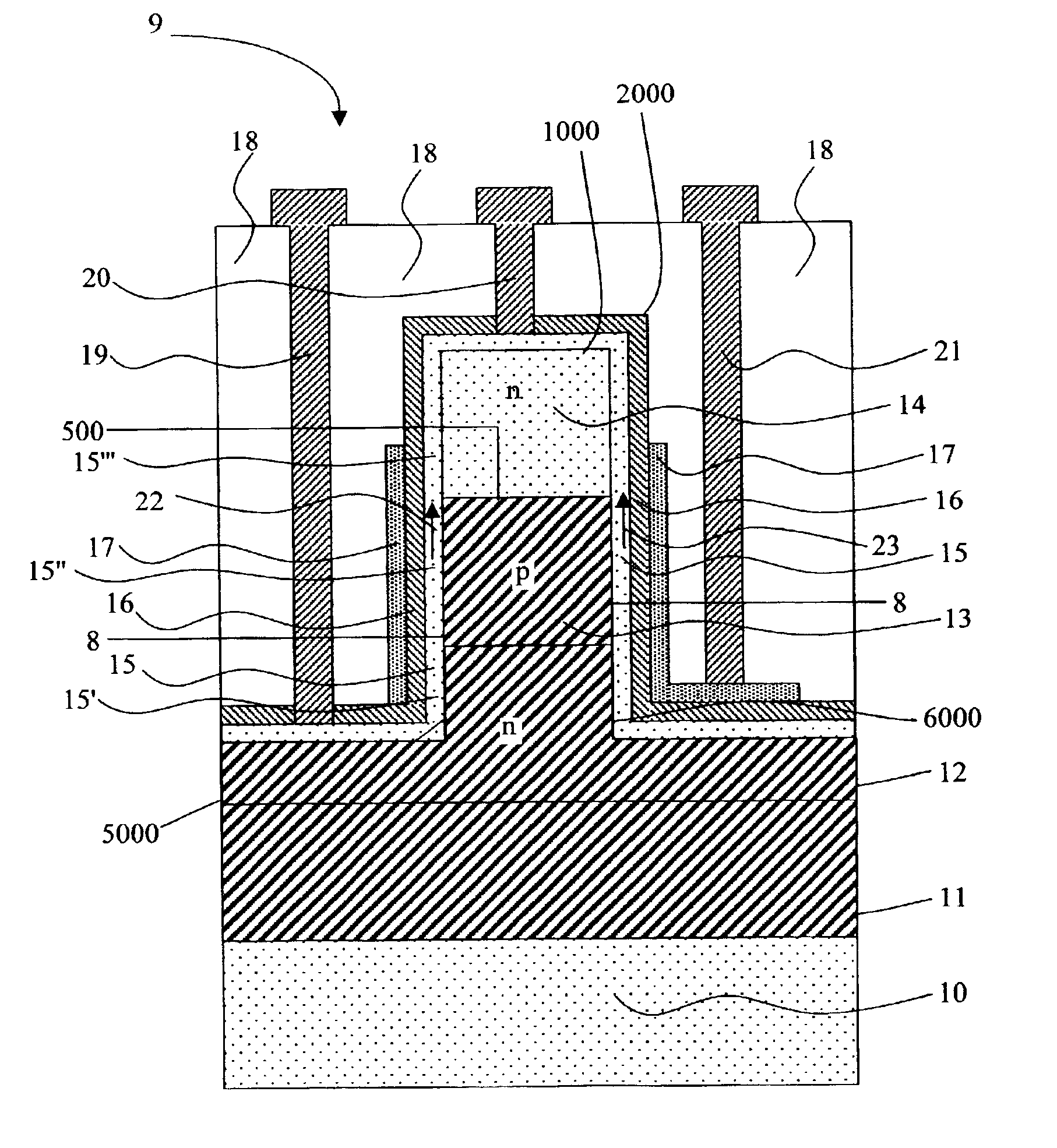
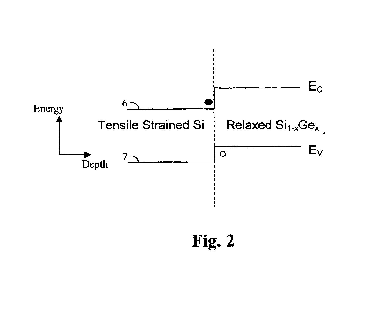
[0029]FIGS. 3 shows a top view of a vertical device structure disclosed in this invention. FIG. 4 shows a cross-sectional view of the It is a SiGe based vertical nMOSFET 9 comprising a vertical mesa, a column, a pedestal, a pillar or a fin comprising several layers, such as a source layer 14, a body layer 13, and a drain layer 12, with a channel layer 15, an insulator layer 16, and a gate electrode layer 17 on the sidewalls of the mesa, column, pedestal, pillar or fin, which may be formed by etching layers 14, 13, and 12. The device has the following structural characteristics:[0030]1) The drain is n+-type relaxed SiGe 12;[0031]2) The body is epitaxial p-type relaxed SiGe 13, and the doping level is adjusted to achieve the desirable threshold voltage;[0032]3) The source is epitaxial n+-type tensile strained Si 14;[0033]4) The channel is epitaxial tensile strained Si 15, and there is no hetero-barrier along the current flow direction shown by arrows 22 and 23. The channel layer 15 f...

fourth embodiment

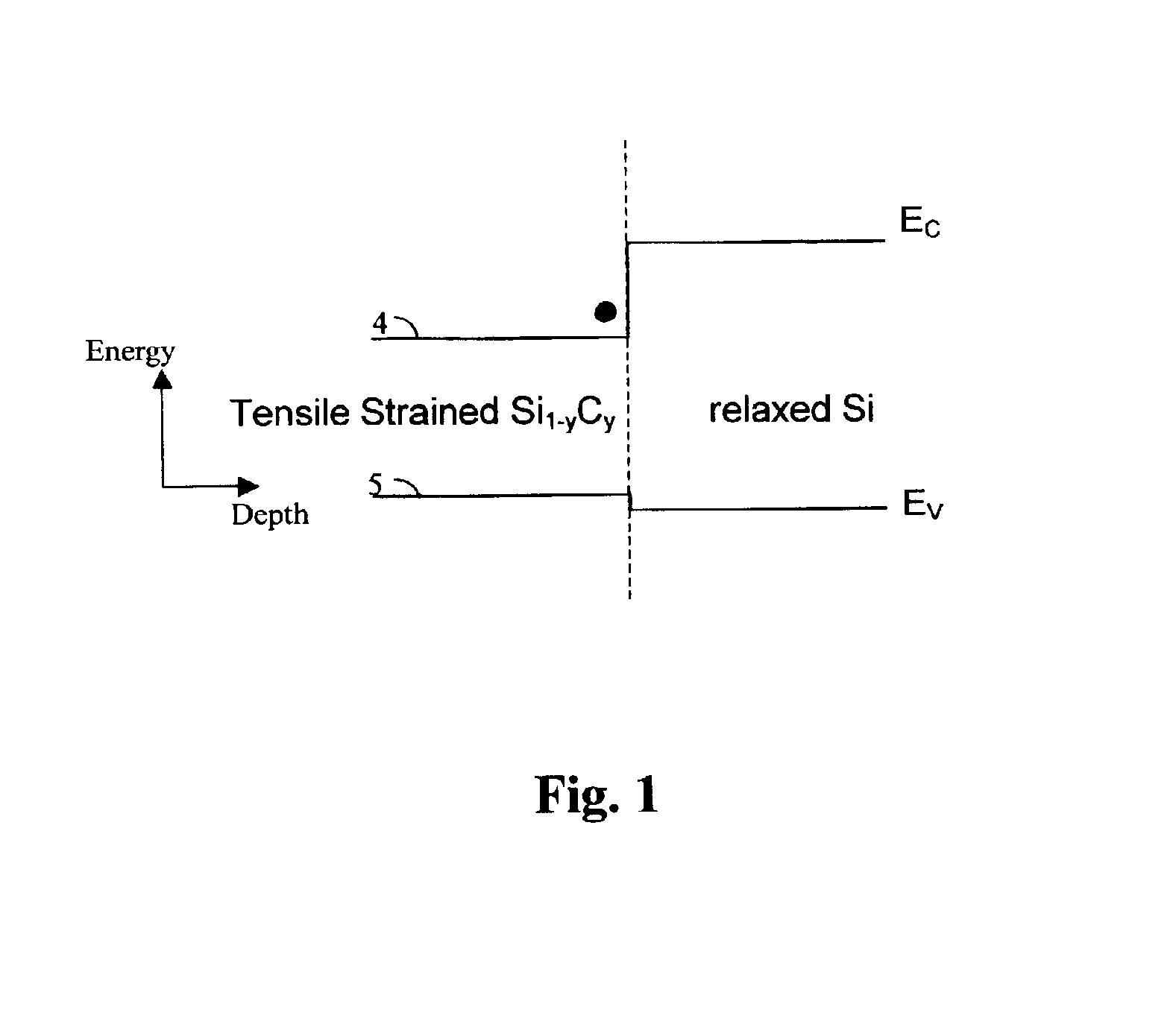
[0041]In order to circumvent this problem, another hetero-material system may be used for nMOSFETs. Tensile strained Si1−x−yGexCy on silicon also has the desired conduction band offset, and in this case it does not require a relaxed SiGe virtual substrate. The cross sectional schematic of the fourth embodiment is shown in FIG. 7 for such a vertical surface channel device 60. The device has the following structure characteristics:[0042]1) The drain is n+-type silicon 62;[0043]2) The body is p-type silicon 63, and the doping level is adjusted to achieve desirable threshold voltage;[0044]3) The source is n+-type tensile strained Si1−x−yGexCy 64;[0045]4) The channel is silicon or strained Si1−a−bGeaCb 65, and there is no hetero-barrier along the current flow direction shown by arrows 72 and 73;[0046]5) A strained Si1−x−yGexCy / Si heterojunction is formed between the source and the body at the interface 600, and preferably, aligned with the source / body metallurgical p / n junction;[0047]6) ...


PUM


Abstract

A method for forming and the structure of a strained vertical channel of a field effect transistor, a field effect transistor and CMOS circuitry is described incorporating a drain, body and source region on a sidewall of a vertical single crystal semiconductor structure wherein a heterojunction is formed between the source and body of the transistor, wherein the source region and channel are independently lattice strained with respect to the body region and wherein the drain region contains a carbon doped region to prevent the diffusion of dopants (boron) into the body. The invention reduces the problem of leakage current from the source region via the heterojunction and lattice strain while independently permitting lattice strain in the channel region for increased mobility via choice of the semiconductor materials.

Description

CROSS REFERENCE TO RELATED APPLICATIONS[0001]This patent application is a continuation-in-part of pending prior U.S. patent application Ser. No. 10 / 364,786, filed Feb. 11, 2003 by Gregory Whittaker et al. for METHOD AND APPARATUS FOR FIXING A GRAFT IN A BONE TUNNEL which patent application is hereby incorporated herein by reference.[0002]This application is cross referenced to U.S. patent application Ser. No. 10 / 463,039 by Q. Ouyang and Jack O. Chu, the inventors herein, filed herewith, entitited “Low Leakage Heterojunction Vertical Transistors and High Performance Devices Thereof” which is directed to a vertical p-channel MOSFET which is incorporated herein by reference and assigned to the assignee herein.[0003]This application is further cross referenced to U.S. patent application Ser. No. 10 / 462,933 by Q. Ouyang and Jack O. Chu, the inventors herein, filed herewith, entitled “High Speed Lateral Heterojunction MISFETS Realized by 2-dimensional Bandgap Engineering and Methods There...

Claims


Application Information

Patent Timeline
Patent Type & Authority Patents(United States)
IPC IPC(8): H01L29/94A61B17/56A61B17/16A61B17/17A61B19/00
CPCH01L29/1054H01L29/778H01L29/7781H01L29/7782H01L29/7789H01L29/7828H01L29/161H01L29/165
Inventor OUYANG, QIQING CHRISTINECHU, JACK OON
Owner GLOBALFOUNDRIES US INC
Why Eureka
Try Eureka