Electromagnetic/circuit co-simulation and co-optimization with parametric layout components

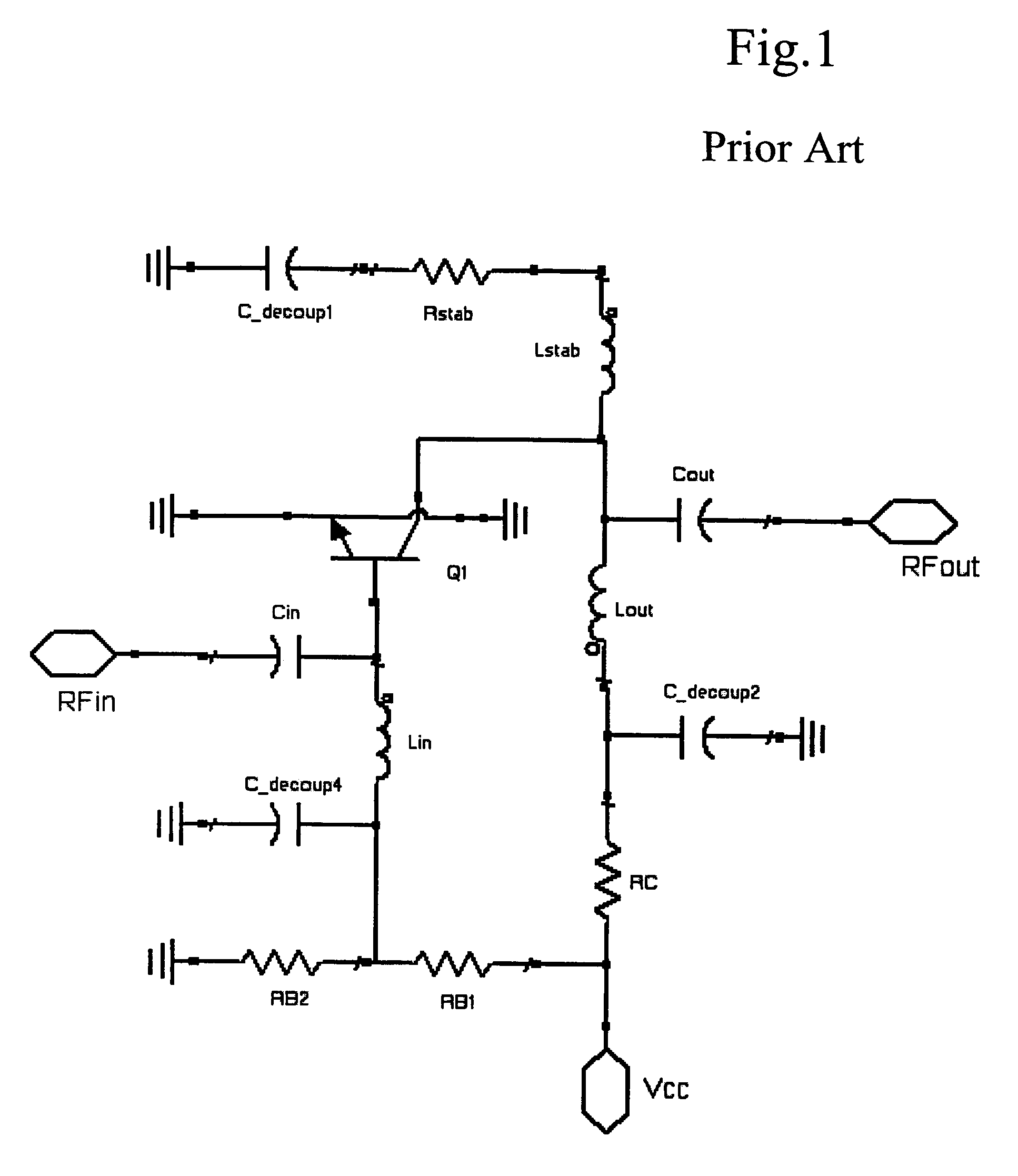
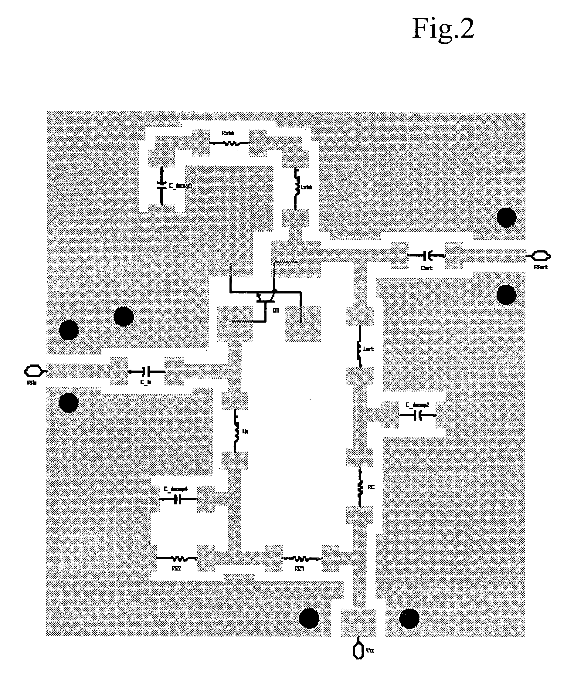
a technology of layout components and circuits, applied in error detection/correction, program control, instruments, etc., can solve problems such as design approaches in common use that do not perform parasitic analysis and physical verification, design flow bottlenecks, and redesign of original circuits, so as to facilitate more extensive use of em simulation and control the amount of cpu processing time

Inactive Publication Date: 2007-04-17
KEYSIGHT TECH
View PDF3 Cites 36 Cited by
  • Summary
  • Abstract
  • Description
  • Claims
  • Application Information

AI Technical Summary

Benefits of technology

[0015]The invention facilitates more extensive use of EM simulation, for example in the characterisation and optimisation of layout interconnects to take proper account of parasitic effects, and at the same time helps to control the amount of CPU processing time that is required.

Problems solved by technology

Yet design approaches in common use do not perform parasitic analysis and physical verification until after attaining the basic prescribed electrical design specifications.
Although there are many benefits to this approach, it also introduces some challenges, especially between design implementation in the circuit domain (schematic) and physical domain (layout).
However, most engineers tend to stay close to the area of knowledge they know well (i.e. schematic circuits), and leave physical design verification to someone else, to be performed later in the design cycle.
This delay in including key parasitic effects in the design process causes design flow bottlenecks, and often, redesign of the original circuit.
Although EM simulators are very successful in providing accurate models for real-life physical effects, their adoption in the electronic design process has been hampered by some significant restrictions, the most important ones being the limited integration in the design framework, their limited performance in relation to the computer resources they require, and high level of expertise required for their effective use.
A major bottleneck in high-frequency design is the time spent transferring design data between independent design tools for EM analysis and verification.
In another step, the EM generated results are manually back-annotated to the original circuit design via black-box representations, a process that is time consuming and cumbersome.
This complicates design analysis, especially when several variations of the physical design effects are under study.
In general, most design bottlenecks occur when transferring the design between the schematic (for circuit performance analysis) and layout (for physical design modelling and verification) to obtain a successful integration of physical parasitics at the schematic level.
Another problem is the prerequisite that the designer using the EM tool must have some understanding of the underlying modelling technology in order to be successful.
However, the partitioning and the circuit description do not always properly account for actual field effects and couplings that occur in the real-world circuit.
However, although in the past decade much progress has been seen in the development of efficient field simulators, accompanied by a very large increase in computer speed and memory, field simulators remain slower relative to circuit simulators.
This lack of speed is especially problematic for activities such as optimization, tuning and yield analysis that require a very large number of circuit evaluations.
Secondly, EM simulators are best suited for the passive linear part of the circuit, and it is much more difficult to include active and non-linear elements which are more easily incorporated in circuit simulation.
However, the speed of the simulation and optimization process critically depends upon the number of data samples to be evaluated and the time needed to solve the EM problem for each selected sample, and this can quickly become problematic.
This makes existing solutions for EM / circuit co-optimization impractical for real-world electronic design work.
While conceptually attractive, the long time required to optimize EM-nonlinear co-simulation is not practical for real-world design” (“The 2001 MEE CAD benchmark: Rat-Race Mixer Characterization”, Microwave Engineering Europe, October 2001).

Method used


Image

  • Electromagnetic/circuit co-simulation and co-optimization with parametric layout components
  • Electromagnetic/circuit co-simulation and co-optimization with parametric layout components
  • Electromagnetic/circuit co-simulation and co-optimization with parametric layout components

Examples


Embodiment Construction

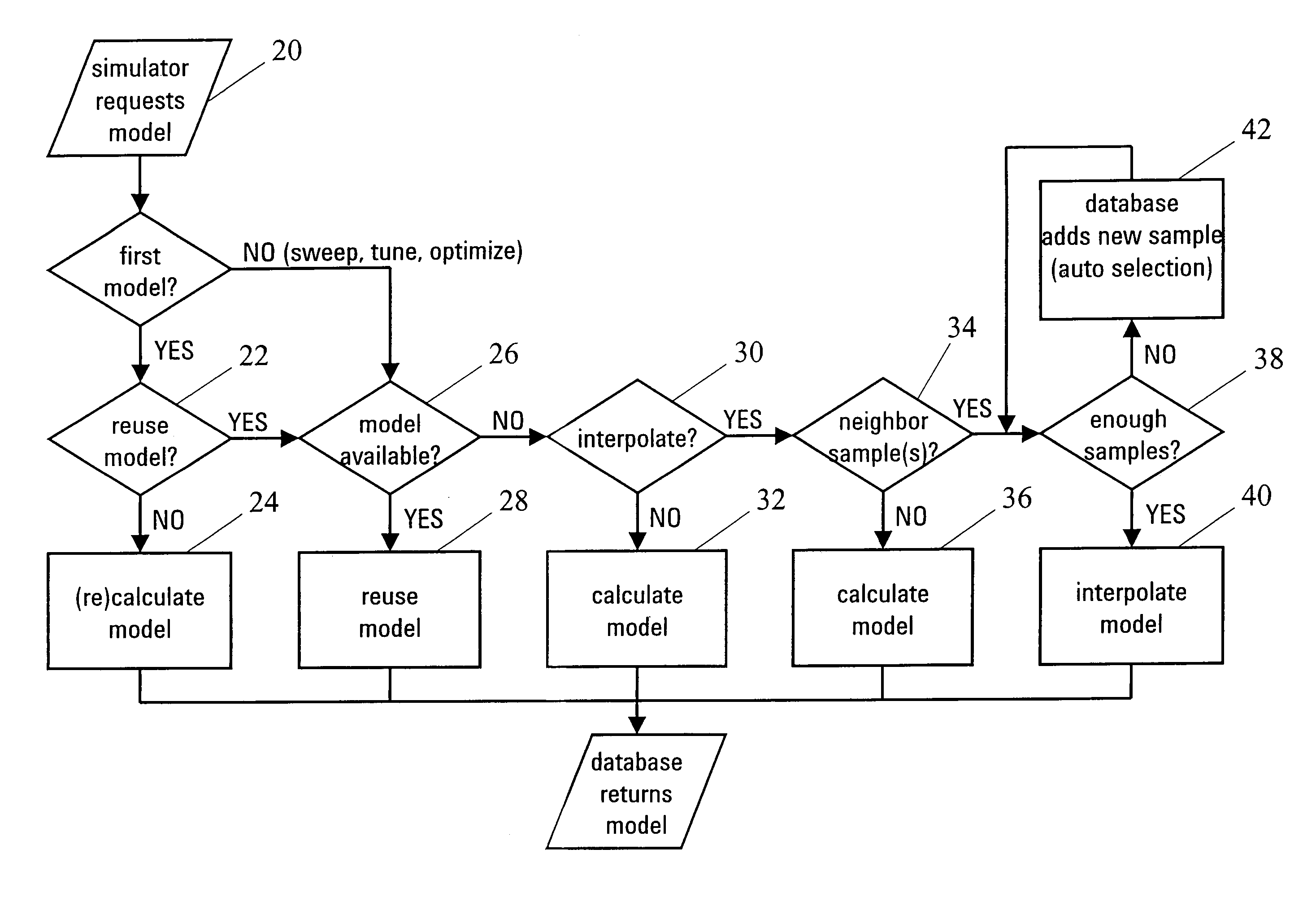
[0031]The invention provides a new concept of “parametric layout components” with an associated EM model database. Parametric layout components allow high-frequency circuit designers to incorporate physical design parasitics at the schematic design level. Once generated, the parametric layout components are available from a components library and are usable together with schematic components for concurrent EM / circuit co-simulation and co-optimization. With parametric layout components, high-frequency designers can start physical design analysis alongside analysis of the circuit's electrical performance, in the same schematic window. In other words, by including layout effects at the same time as electrical performance, designers can include real-world effects as they develop their circuits. This new concept goes beyond incremental design flow improvements, and introduces a new paradigm for tackling real-world physical design challenges.

[0032]Each parametric layout component has an a...


PUM


Abstract

Simulation of electromagnetic characteristics of an electrical circuit uses netlist data defining component instances, including layout component instances, and their topological interconnection in an electrical circuit. A circuit simulation is performed using the netlist data, involving use of a model for each layout component instance. An attempt is made to retrieve an existing simulation model of the layout component instance from a database of such layout component simulation models. If no suitable simulation model can be found in the database, an attempt is made to interpolate a new simulation model from among existing simulation models in the database. If interpolation is determined not to be feasible, then an electromagnetic simulation of the layout component instance is performed to develop a new electromagnetic simulation model. This new model is used in the circuit simulation, and added to the database for future use.

Description

TECHNICAL FIELD[0001]This invention relates to electromagnetic / circuit co-simulation and co-optimization with parametric layout components.BACKGROUND ART[0002]Technological advances in wireless and wireline data communications have resulted in communications systems and integrated circuits that operate at very high RF, microwave and millimetre-wave frequencies. At these high frequencies the physical effects of metal interconnections between functional components play a major role in the electronic circuit performance. Accurate prediction of the circuit performance before fabrication, by means of electronic design automation (EDA) tools, has become essential for shortening design cycles and lowering engineering cost. Incorporating real-world physical effects in the early stages of the electronic design process is essential for achieving design success with very few design iterations. Yet design approaches in common use do not perform parasitic analysis and physical verification until...

Claims


Application Information

Patent Timeline
Patent Type & Authority Patents(United States)
IPC IPC(8): G06F17/50H05K9/00
CPCG06F17/5036G06F30/367
Inventor SERCU, JEANNICKDEMUYNCK, FILIPLEE, HEE-SOOAL-KURAN, SHIHABHAMMADI, SAMIRHUANG, CHUN-WEN PAUL
Owner KEYSIGHT TECH
Why Eureka
Try Eureka