Method for manufacturing semiconductor device

a manufacturing method and semiconductor technology, applied in the direction of instruments, electrical appliances, optics, etc., can solve the problems of increased manufacturing cost, reduced longitudinal length, and reduced heat resistance of materials, so as to reduce heat resistance temperature, reduce cost, and improve heat resistance.

Inactive Publication Date: 2007-05-01
SEMICON ENERGY LAB CO LTD
View PDF30 Cites 16 Cited by
  • Summary
  • Abstract
  • Description
  • Claims
  • Application Information

AI Technical Summary

Benefits of technology

[0016]Because the present invention having the above structure is performed in normal pressure or under reduced pressure, continuous processing can be performed by using a load lock mechanism, and it can be realized in lower cost. According to the present invention, the contact hole can be filled by the short heat treatment at; therefore, a wiring having a favorable coverage can be formed in an organic insulating film having lower heat resistance temperature. Further, by using the organic insulating film with lower dielectric constant, a wiring capacity can be reduced and multilayer wiring can be obtained, thereby a semiconductor device with higher performance and advanced function can be realized.

Problems solved by technology

However, the reduction in a longitudinal length has not realized due to keep lower resistance.
However, since the organic material has lower heat resistance, it can be resolved and damaged according to the treatment temperature.
Further, a manufacturing cost has been increased since it takes time to carry the substrate out or into of each the equipment.

Method used


Image

  • Method for manufacturing semiconductor device
  • Method for manufacturing semiconductor device
  • Method for manufacturing semiconductor device

Examples


embodiment 1

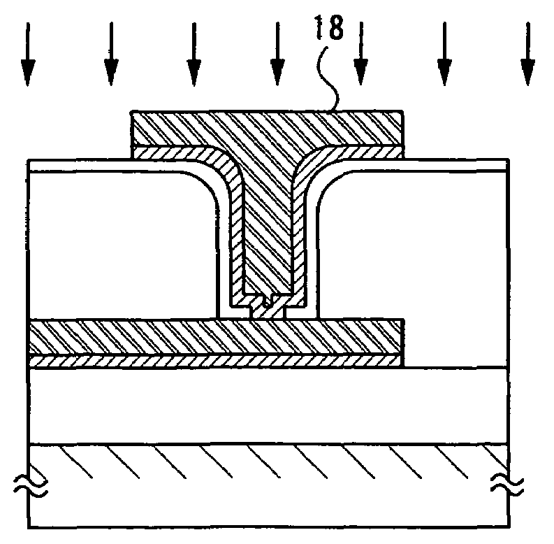
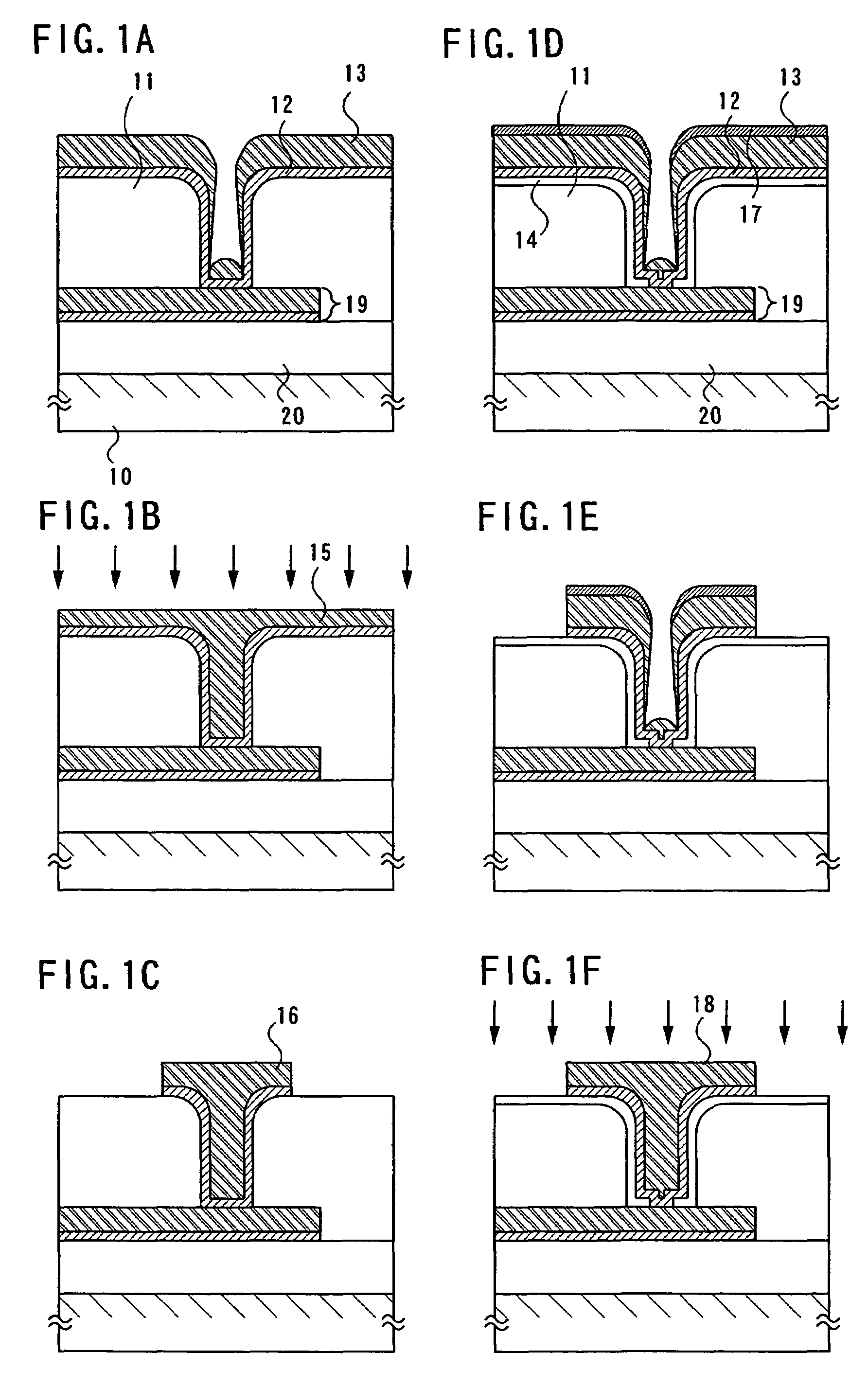
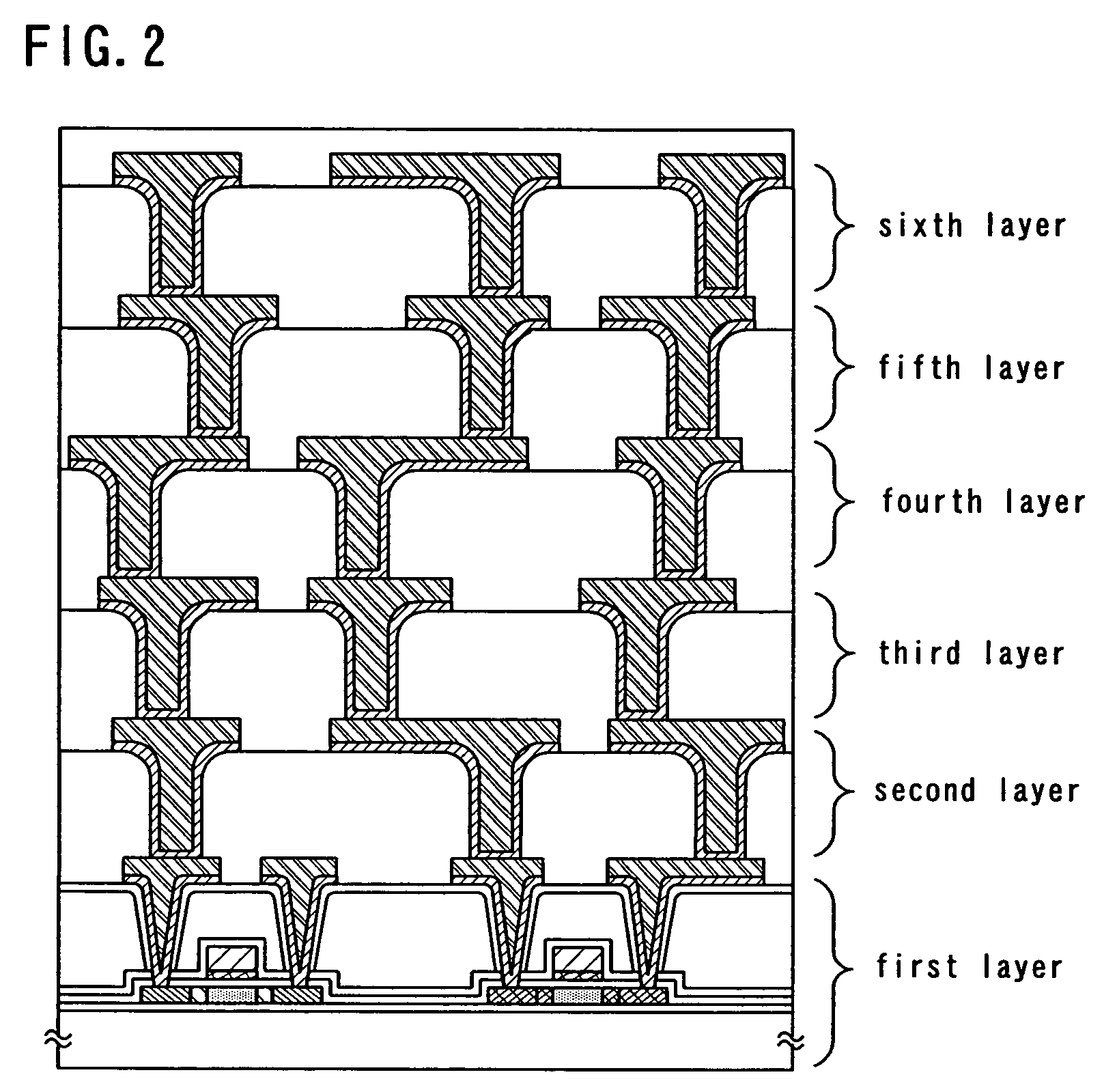
[0049][Embodiment 1]

[0050]A embodiment of the present invention is described with reference to FIG. 2.

[0051]FIG. 2 is a cross sectional view of a semiconductor device in which six layers is formed over a substrate 10. An example that the first layer is a semiconductor element (here, only a thin film transistor), and the second to the sixth layers are wirings is shown.

[0052]When such the multilayer wiring is formed, the component ratio of one kind or plural kinds of conductive materials selected from the group consisting of Ge, Sn, Ga, Zn, Pb, In, or Sb is preferably increased from the lower layer toward the upper layer. Accordingly, the treatment temperature in the reflow step can be reduced from the lower layer toward the upper layer.

[0053]A semiconductor device including the multilayer wiring is preferably used for the function circuit in which a plurality of semiconductor elements such as CPU is required to be incorporated. Temporarily, in the case of not forming the multilayer w...

embodiment 2

[0056][Embodiment 2]

[0057]In this embodiment, a manufacturing step of forming an n-channel type transistor and a p-channel type transistor over the same substrate is described with reference to the drawings.

[0058]An insulating film including silicon such as a silicon nitride oxide film or a silicon oxynitride film is formed into a single layer or a laminated layer over a substrate 300 having an insulating surface as a base film 302 by a publicly known method (plasma CVD or the like)

[0059]Next, an amorphous semiconductor film is formed with a thickness of 25 nm to 100 nm by a publicly known method (sputtering, LPCVD, plasma CVD, or the like). Subsequently, the amorphous semiconductor film is crystallized by a publicly known method for crystallization (a laser crystallization method, a thermal crystallization method using RTA or an annealing furnace, a thermal crystallization method using a metal element which promotes the crystallization, or the like). Thus the obtained crystalline s...

embodiment 3

[0075][Embodiment 3]

[0076]The embodiment mode of the present invention is described with reference to FIGS. 5A to 5C. In this embodiment, a panel mounted with a pixel portion, a driver circuit for controlling the pixel portion, a memory and CPU over the same surface is described. FIG. 5A is a top view of a display panel formed by sealing substrate where a TFT is formed with a sealant. FIG. 5B is a cross-sectional view taken along the line B–B′ of FIG. 5A, and FIG. 5C is a cross-sectional view taken along the line A–A′ of FIG. 5A.

[0077]FIG. 5A shows appearance of the panel. The panel comprises a pixel portion 401 in which plural pixels are arranged in matrix over a substrate 400, and a signal line driver circuit 402 and a scanning line driver circuit 403 for controlling the pixel portion 401. And, the sealant 407 is provided so as to surround them. A counter substrate 409 may be provided for only over the pixel portion 401, the drive circuits 402 and 403, or for the entire surface. H...


PUM

PropertyMeasurementUnit
heat resistant temperatureaaaaaaaaaa
relative dielectric constantaaaaaaaaaa
thicknessaaaaaaaaaa

Abstract

A method for manufacturing a semiconductor device in which lower cost can be realized, a wiring with favorable coverage can be formed in a contact hole having a large aspect ratio, wiring capacitance can be reduced and a multilayer wiring can be formed, can be provided. In order to obtain the semiconductor device, the following steps are required; forming a first conductive film which serves as a barrier so as to be in contact with an organic insulating film with an opening portion formed; forming a second conductive film including aluminum so as to be in contact with the first conductive film; or forming a nitride film so as to be in contact with the organic insulating film with the opening portion formed; patterning the nitride film; forming a first conductive film which serves as a barrier so as to be in contact with the nitride film; forming a second conductive film including aluminum so as to be in contact with first conductive film; and thereafter selectively performing a heat treatment under reduced pressure or in normal pressure, and flattening the second conductive film.

Description

BACKGROUND OF THE INVENTION[0001]1. Field of the Invention[0002]The present invention relates to a method for manufacturing a semiconductor device, which comprises a step for manufacturing a wiring by a reflow method.[0003]2. Description of the Related Art[0004]Recently, development for a highly integrated, high speed, and miniaturized semiconductor device has been advanced. According to the miniaturization, the length of the side can be reduced to approximately 70%. However, the reduction in a longitudinal length has not realized due to keep lower resistance. Therefore, a technique to form the wiring in a narrow and deep hole that has a large aspect ratio has been required. As a metal embedded technique by which a metal material is embedded in the trench which is formed in the insulating film in advance, metal CVD or the reflow method has been developed. The reflow method is a considerably promising technique since it can be performed in lower cost.[0005]In order to obtain a higher...

Claims


Application Information

Patent Timeline
Patent Type & Authority Patents(United States)
IPC IPC(8): H01L21/44G02F1/1362H01L21/768
CPCG02F1/136227H01L21/76843H01L21/76882
Inventor YAMAZAKI, SHUNPEIYAMAGUCHI, TETSUJIISOBE, ATSUO
Owner SEMICON ENERGY LAB CO LTD
Why Eureka
Try Eureka