Optical waveguide device, coherent light source using the same and optical apparatus having the same

a technology of optical waveguide and light source, which is applied in the direction of instruments, semiconductor lasers, optical elements, etc., can solve the problems of crystal deformation, reduced resistance to optical damage, and inability to use the structure of optical waveguide devices, etc., and achieves high efficiency and stable

Active Publication Date: 2007-06-26
PANASONIC CORP +1
View PDF14 Cites 18 Cited by
  • Summary
  • Abstract
  • Description
  • Claims
  • Application Information

AI Technical Summary

Benefits of technology

[0014]In view of the above-stated problems, an object of the present invention is to provide an optical waveguide device according to the present invention, a coherent light source using the same and an optical apparatus having the same, which will provide a short wavelength light source that is highly efficient and stable.
[0016]It is also preferable that the domain-inverted structure is formed by applying voltage in a polarization direction of the substrate. Thereby, as a change in composition of the crystal will not occur, an optical waveguide device with high efficiency and high output can be realized.
[0018]It is also preferable that an offcut angle of the substrate is inclined in a range of 1° to 10° with respect to the substrate surface. Thereby, reflectance from the DBR grating is increased.
[0019]It is also preferable that the substrate has an optical substrate as a thin film bonded to one face of the substrate via an adhesive layer. Thereby, reflectance from the DBR grating is increased.
[0020]It is also preferable that a convex is formed on at least either the surface or back face of the substrate, and that the domain-inverted structure is formed in stripes on the convex. Thereby, a ridge-type optical waveguide device is provided, where crystal distortion formed will not be influenced by the domain inversion, and thus the change in refractive index can be maintained. As a result, a high DBR reflection can be realized, and the DBR grating has a high efficiency.

Problems solved by technology

However, such a change in crystal composition can result in degradation of the crystal itself, and it may cause problems such as degradation of the crystal and reduction of resistance to optical damage.
Thus such a structure cannot be used for an optical waveguide device that enables transmission of high-output light at high efficiency.
However, the domain inversion caused by the Ti diffusion on the LiNbO3 substrate will not provide a sufficient depth of the domain inversion.
Particularly, it is difficult to form a domain-inverted structure having a period of not more than 3 μm, which is required for a wavelength of about 400 nm or less.
Moreover, when Ti is diffused, impurity concentration in the optical waveguide increases and the resistance to optical damage will deteriorate.
As a result, the output may be unstable at the time of output that is as high as at least several milliwatts.
However, since the Rb as an impurity enters the crystal, it will be difficult to provide high output, similarly to the case of Ti diffusion.
Furthermore, since a large difference in the grating constants is provided between the ion exchange portion and non-exchange portion due to the ion exchange with the Rb, distortion or the like may occur in the crystal at the inverted part, thereby increasing a loss in the transmission in the optical waveguide.
However, since there is no change in the crystal composition, changes in refractive index will not occur and thus it cannot be used for a DBR grating.

Method used


Image

  • Optical waveguide device, coherent light source using the same and optical apparatus having the same
  • Optical waveguide device, coherent light source using the same and optical apparatus having the same
  • Optical waveguide device, coherent light source using the same and optical apparatus having the same

Examples


first embodiment

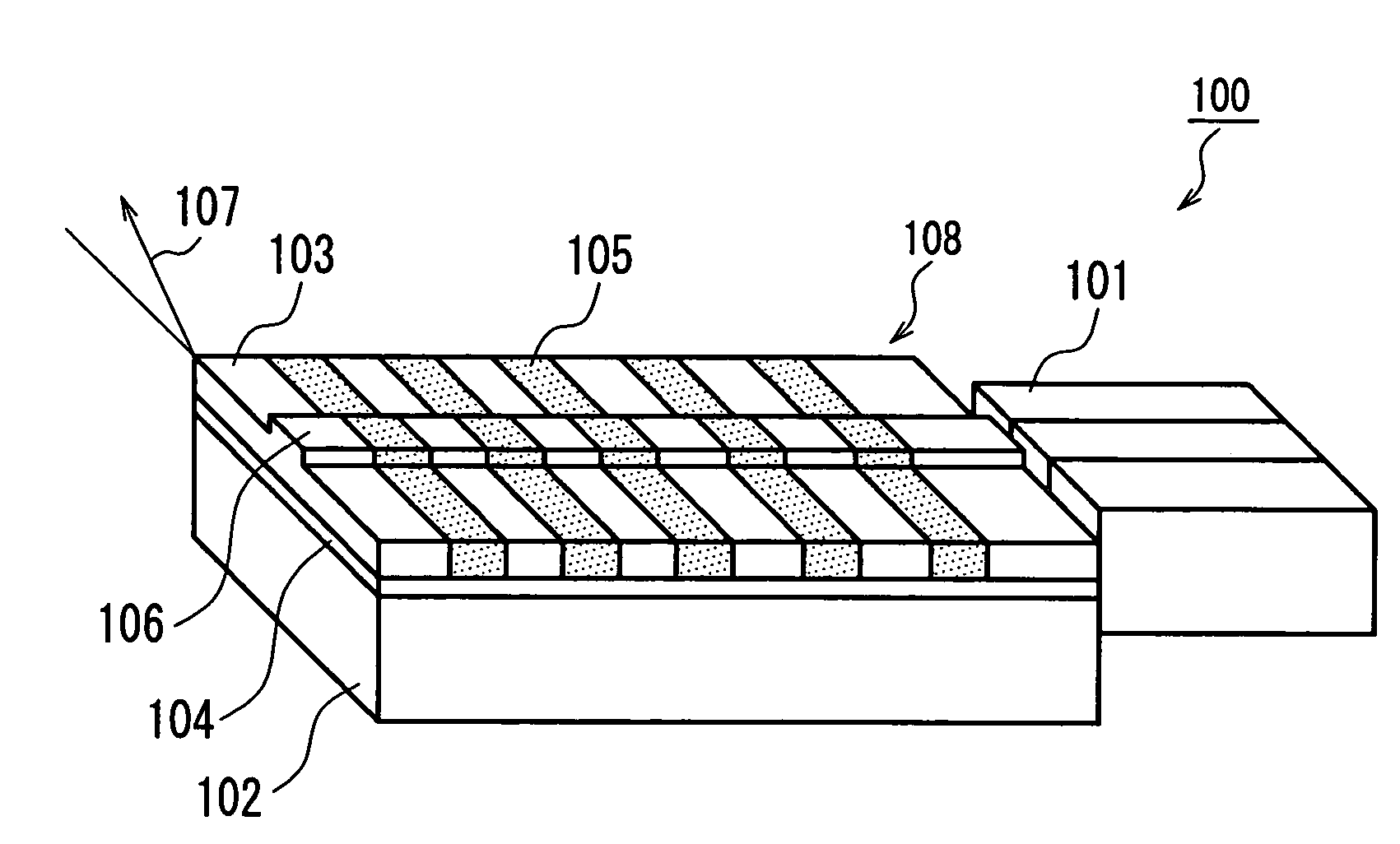
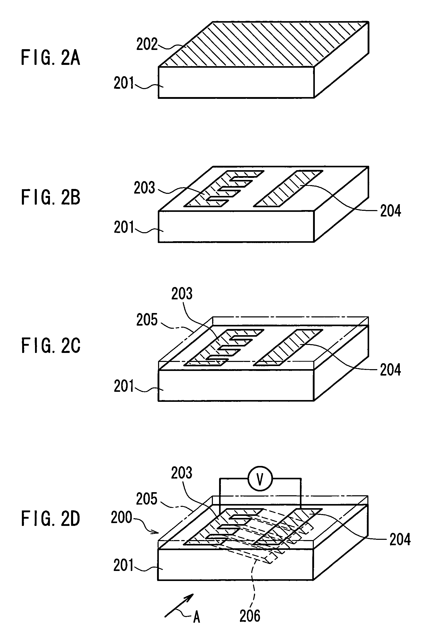
[0041]An optical waveguide device according to a first embodiment of the present invention and a coherent light source using the same will be described below. FIG. 1 is a diagram showing a coherent light source using an optical waveguide device according to the first embodiment of the present invention. The coherent light source 100 in the first embodiment has a semiconductor laser 101 and an optical waveguide device 108 as an optical wavelength converter.

[0042]The optical waveguide device 108 is configured by adhering an offcut thin film layer 103 of a Mg-doped LiNbO3 crystal onto a LN substrate 102 via a bonding layer 104. On the thin film layer 103, a striped convex 106 is formed. The optical waveguide device 108 having this convex 106 as a ridge waveguide is a so-called ridge-type waveguide structure. On the thin film layer 103, a periodic periodically domain-inverted region 105 is formed. Since the thin film layer 103 is made of an offcut substrate, a polarization direction 107...

second embodiment

[0082]The description below refers to an optical waveguide device according to a second embodiment of the present invention and a coherent light source using the same. FIG. 5 is a diagram showing a coherent light source using an optical waveguide device according to the second embodiment.

[0083]A coherent light source 100a according to the second embodiment as shown in FIG. 5 has an optical waveguide device 108a in place of the optical waveguide device 108 of the coherent light source in the first embodiment, and a domain-inverted region 105 of this optical waveguide device 108a is separated into a DBR portion 112 and a wavelength-converting portion 111. The semiconductor laser 101 is a Fabry-Perot AlGaAs semiconductor laser similarly to the first embodiment. However, unlike the first embodiment, the domain-inverted region 105 has a domain-inverted period of about 2.7 μm and a phase matching wavelength of about 810 nm.

[0084]Both the DBR portion 112 and the wavelength-converting porti...

third embodiment

[0097]An embodiment of an optical apparatus of the present invention will be described below. Examples of the optical apparatus include an optical pickup apparatus. FIG. 6 is a schematic view showing a configuration of an optical pickup system according to a third embodiment. An optical pickup apparatus 400 according to the third embodiment has a coherent light source 401, lenses 402 and 404 as convergent optical systems, a beam splitter 403 and a photodetector 405. For the coherent light source 401, any of the coherent light sources 100, 300 and 100a in the first and second embodiments as illustrated in FIGS. 1, 4 and 5 can be used.

[0098]As shown in FIG. 6, a light beam 407 emitted from the coherent light source 401 passes through the lens 402 as an optical convergent system, the beam splitter 403 and the lens 404 as an optical convergent system so as to be converged on the surface of an optical disk 406. The thus converged light beam is reflected on the surface of the optical disk...


PUM

PropertyMeasurementUnit
offcut angleaaaaaaaaaa
Bragg reflection wavelengthaaaaaaaaaa
phase matching wavelengthaaaaaaaaaa

Abstract

An optical waveguide device has a substrate composed of a nonlinear optical material and a periodically domain-inverted structure having the same composition as the nonlinear optical material, where the domain-inverted structure has a refractive index distribution relying on the domain-inverted structure.

Description

TECHNICAL FIELD[0001]The present invention relates to an optical waveguide device used in the fields of optical information processing and optical application measurement control, a coherent light source using the same and an optical apparatus having the same.BACKGROUND ART[0002]For an apparatus for recording and reproducing optical information, a high density can be realized by using a light source having a shorter wavelength. For example, while near infrared light of 780 nm is used for a widespread compact disk apparatus, a red semiconductor laser of 650 nm is used for a digital versatile disk (DVD) realizing a higher density information reproduction. Furthermore, for realizing a high density next-generation optical disk apparatus, a blue laser light source having a shorter wavelength has been developed keenly. For example, a wavelength converter using a nonlinear optical material has been developed for a small and stable blue laser light source.[0003]For example, a QPM (quasi-pha...

Claims


Application Information

Patent Timeline
Patent Type & Authority Patents(United States)
IPC IPC(8): G02B6/10G02F1/35H01S3/10G02F1/377G02F1/355
CPCG02F1/3558G02F1/3775G02F2201/30H01S5/141H01S3/109
Inventor MIZUUCHI, KIMINORIYAMAMOTO, KAZUHISAIMAEDA, MINORUKAWAGUCHI, TATSUOYOSHINO, TAKASHI
Owner PANASONIC CORP
Why Eureka
Try Eureka