

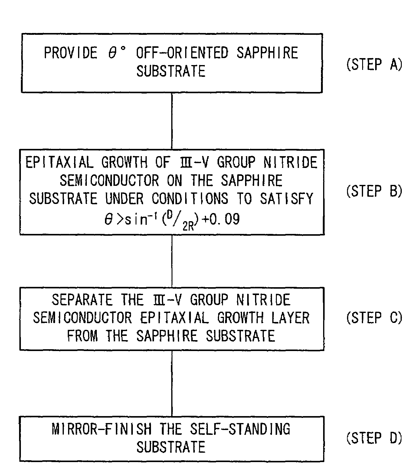
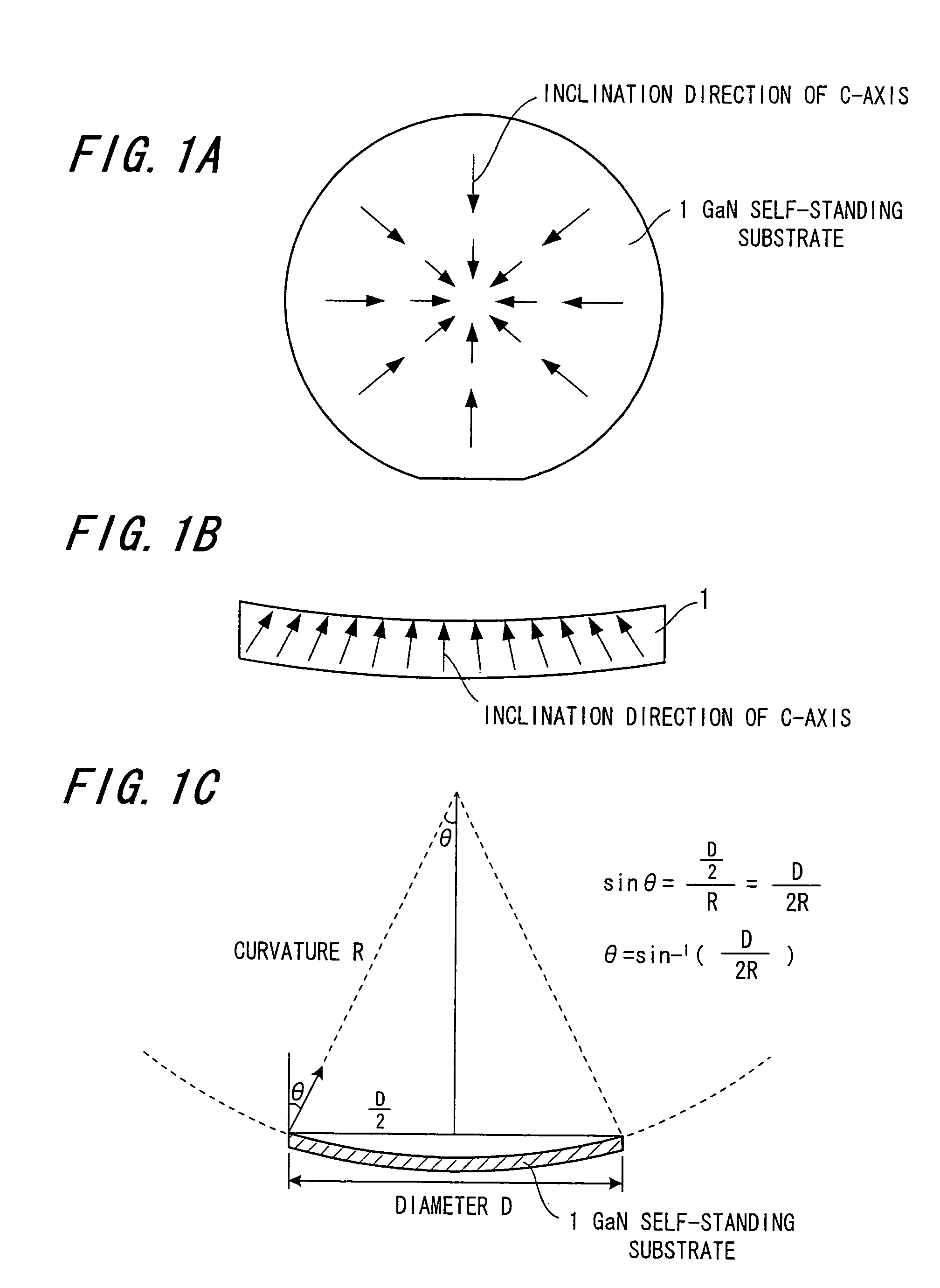
III-V group nitride system semiconductor self-standing substrate, method of making the same and III-V group nitride system semiconductor wafer
a nitride system and semiconductor technology, applied in the direction of polycrystalline material growth, chemically reactive gas growth, crystal growth process, etc., can solve the problems of difficult to grow a bulk crystal of nitride system semiconductor, number of dislocations (defects) must be generated in grown crystals, and difficult to flatten the surface morphology. , to achieve good flatness, uniformity and reproducibility, good flatness, good responsibility
- Summary
- Abstract
- Description
- Claims
- Application Information
AI Technical Summary
Benefits of technology
Problems solved by technology
Method used
Image

Examples
example 1
(Manufacture of GaN Self-standing Substrate by VAS)
[0109]Referring to FIGS. 4A to 4G, the manufacture of a GaN self-standing substrate by the VAS method will be explained below.
[0110]At first, a commercially-available single-crystal sapphire C-face substrate 21 with a diameter of 2 inches is provided that is off-oriented 0.25 degrees in the m-axis direction (FIG. 4A).
[0111]Then, a 300 nm undoped GaN layer 22 is grown on the sapphire substrate 21 by MOVPE using TMG, NH3 as raw materials (FIG. 4B). Then, a 20 nm Ti film 23 is deposited on the GaN epi-substrate (FIG. 4C), entered into an electric oven, and heated at 1050° C. for 20 min in H2 flow with 20% NH3 mixed therein. Thereby, the Ti film 23 is processed into a mesh-like slotted TiN layer 25 and simultaneously the GaN layer 22 is processed into a void-formed GaN layer 24 (FIG. 4D).
[0112]This is entered in an HVPE furnace, and then a 700 μm GaN layer 26 is deposited (FIG. 4E). NH3 and GaCl are used raw materials and mixed gas of N...
example 2
(Formation of GaN Layer on GaN Self-standing Substrate)
[0120]As shown in FIG. 7, a 2 μm Si-doped GaN layer 40 is grown on the GaN self-standing substrate 30 manufactured in Example 1 by MOVPE. The growth pressure of GaN layer 40 is atmospheric pressure and the growth temperature of self-standing substrate 30 is 1100° C. TMG is used as III group raw material, NH3 as V group material, and monosilane as dopant. The carrier gas is mixed gas of hydrogen and nitrogen. The growth rate of crystal is 4 μm / h, and target carrier concentration of epi-layer is 2×1018 cm−3.
[0121]The surface of GaN layer 40 obtained is observed by Nomarski microscope. Although in most areas is observed a linear morphology that is assumed to be formed due to step bunching, only in a limited area is observed a region A that hexagonal uneven patterns of about 5 to 20 μm are collected. FIG. 8 shows the position of region A.
[0122]As the result of measuring the inclination of crystal C-axis inside and outside the region...
example 3
(Manufacture of GaN Self-standing Substrate by VAS)
[0123]In analogy with Example 1, a GaN self-standing substrate is manufactured by the VAS method as shown in FIGS. 4A to 4G.
[0124]At first, a commercially-available single-crystal sapphire C-face substrate 21 with a diameter of 2 inches is provided that is off-oriented 0.30 degrees in the m-axis direction (FIG. 4A).
[0125]Then, a 300 nm undoped GaN layer 22 is grown on the sapphire substrate 21 by MOVPE using TMG, NH3 as raw materials (FIG. 4B). Then, a 20 nm Ti film 23 is deposited on the GaN epi-substrate (FIG. 4C), entered into an electric oven, and heated at 1050° C. for 20 min in H2 flow with 20% NH3 mixed therein. Thereby, the Ti film 23 is processed into a mesh-like slotted TiN layer 25 and simultaneously the GaN layer 22 is processed into a void-formed GaN layer 24 (FIG. 4D).
[0126]This is entered in an HVPE furnace, and then a 700 μm GaN layer 26 is deposited (FIG. 4E). NH3 and GaCl are used raw materials and N2 is used as ca...
PUM
| Property | Measurement | Unit |
|---|---|---|
| off-angle | aaaaa | aaaaa |
| thickness | aaaaa | aaaaa |
| thickness | aaaaa | aaaaa |
Abstract
Description
Claims
Application Information