Manufacturing method of semiconductor device

a manufacturing method and semiconductor technology, applied in the direction of semiconductor/solid-state device details, solid-state diffusion coating, coating, etc., can solve the problems of increasing electrical resistance, decreasing the adhesion between the copper interconnection and the copper-diffusion prevention film formed, and the conventional techniques described above, so as to prevent the increase of electrical resistance and reduce the effect of resistan

Inactive Publication Date: 2007-09-11
RENESAS ELECTRONICS CORP
View PDF14 Cites 9 Cited by
  • Summary
  • Abstract
  • Description
  • Claims
  • Application Information

AI Technical Summary

Benefits of technology

[0027]Further, in the afore-mentioned conventional techniques, even if the treatment is conducted in a plasma atmosphere with a high reducing capability, a copper oxide film cannot help remaining in part. As against this, in the present invention, since the nitriding treatment is applied to a clean copper surface where no copper oxide film remains, the film thickness and the film quality of a CuN film which is formed by the nitriding treatment can be made uniform and, herewith, the film thickness of a copper silicide layer to be formed in the copper interconnection becomes uniform. As a result, the following effects can be attained.
[0028]First, the increase in electrical resistance which may be brought about by oxidation of the copper-containing film surface can be suppressed. In the afore-mentioned manufacturing methods, a protective film made of CuN is homogeneously formed to an uniform thickness over the copper-containing film so that a clean copper-containing metal surface where no copper oxide film is formed is directly covered with the protective film. This protects copper from oxidation with effect in the subsequent steps, and prevents the electrical resistance from increasing.
[0029]Secondly, the interconnection lifetime is lengthened. In the afore-mentioned manufacturing methods, CUN is formed, while the nitriding treatment is being applied to the surface of the copper-containing film, and once a copper-diffusion prevention film comprising silicon is formed, this CuN restrains silicon from diffusing into the copper-containing film. However, CuN does not cut off the silicon diffusion completely, and a small amount of silicon passes through CuN and reaches inside of the copper-containing film to form a thin copper silicide layer in the vicinity of the surface of the copper-containing film. As described above, the protective film made of CUN is homogeneously formed to a uniform thickness so that the silicide layer formed thereunder is a thin layer, homogeneous and having a uniform thickness. The formation of such a silicide layer is considered to be the cause for lengthening of the interconnection lifetime. A silicide layer of this sort can be also formed by the step of forming a silicon nitride film 18, in the method described in the BACKGROUND, referring to FIG. 5. However, because silicon nitride, in this instance, is deposited without a copper nitride layer being formed, silicon that is the very constituting material for silicon nitride diffuses into the copper interconnection, excessively, and a thick silicide layer is formed, causing a problem of the increase in interconnection resistance and contact resistance. Meanwhile, in the afore-mentioned method with a reducing plasma treatment, the formation of a silicide layer itself is considered to be suppressed. Unlike these conventional techniques, in the present invention, because a CuN layer, capable to restrain silicon diffusion appropriately, is formed, a silicide layer can be formed homogeneously and uniformly to a thin film thickness. This enables both objects, an improvement of the interconnection lifetime and a lowering of the electrical resistance, to be achieved together.
[0030]Thirdly, because the copper-diffusion prevention film can be formed homogeneously and with its film thickness well under control, the degradation of the copper-containing film in the subsequent steps can be prevented from occurring. For instance, when the present invention is applied to a method of forming a copper interc

Problems solved by technology

However, conventional techniques described above have the following problems.
During -the transfer, the wafer may be exposed to the air so that the copper surface therein may be reoxidized, leading to a problem of the increase in electrical resistance and the decrease in adhesion between the copper interconnection and the copper-diffusion prevention film formed thereon.
Meanwhile, although a method with a reducing plasma treatment can control the increase in resistance in a certain degree, the method brings about another problem of the decrease in interconnection lifetime.
To remove the copper oxide film thoroughly by the plasma treatment, it is neces

Method used


Image

  • Manufacturing method of semiconductor device
  • Manufacturing method of semiconductor device
  • Manufacturing method of semiconductor device

Examples


example 1

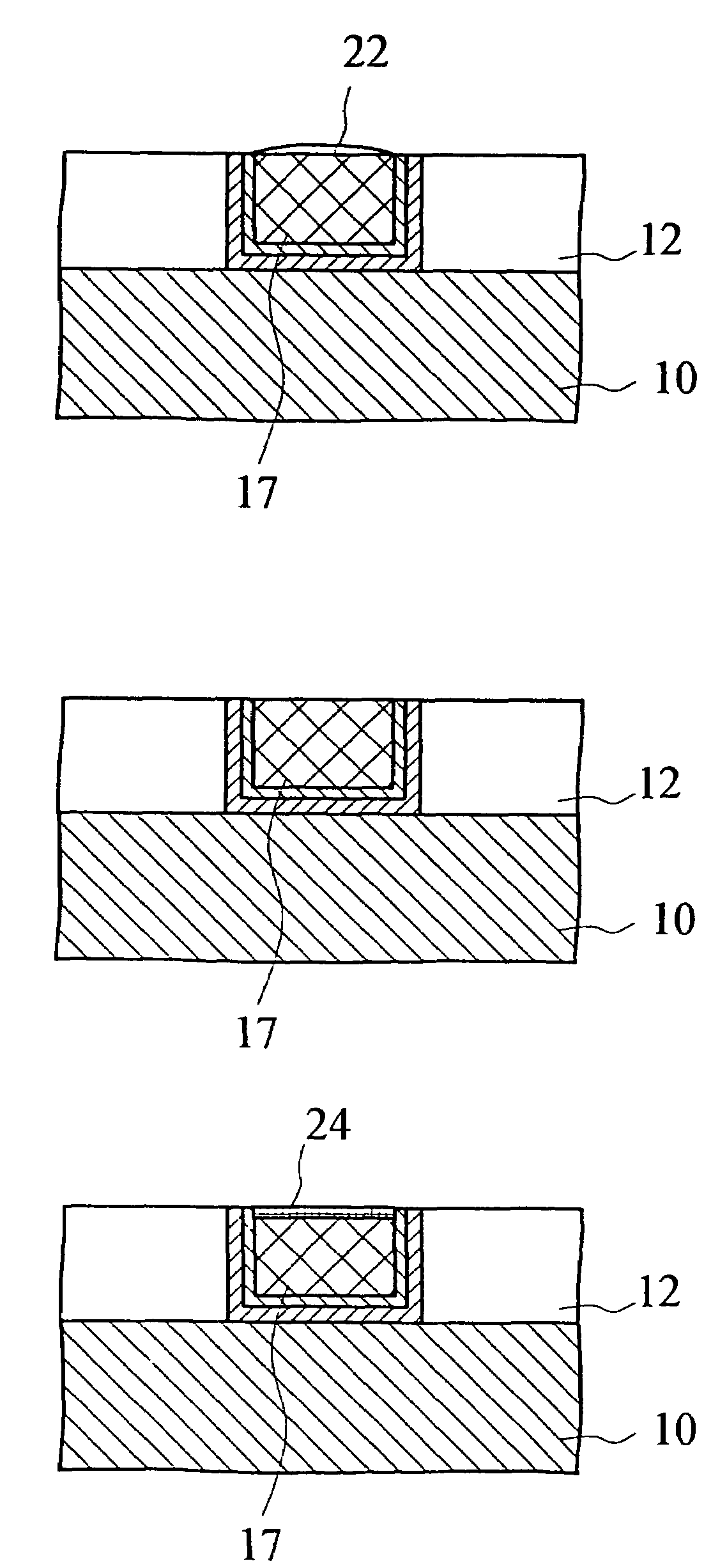
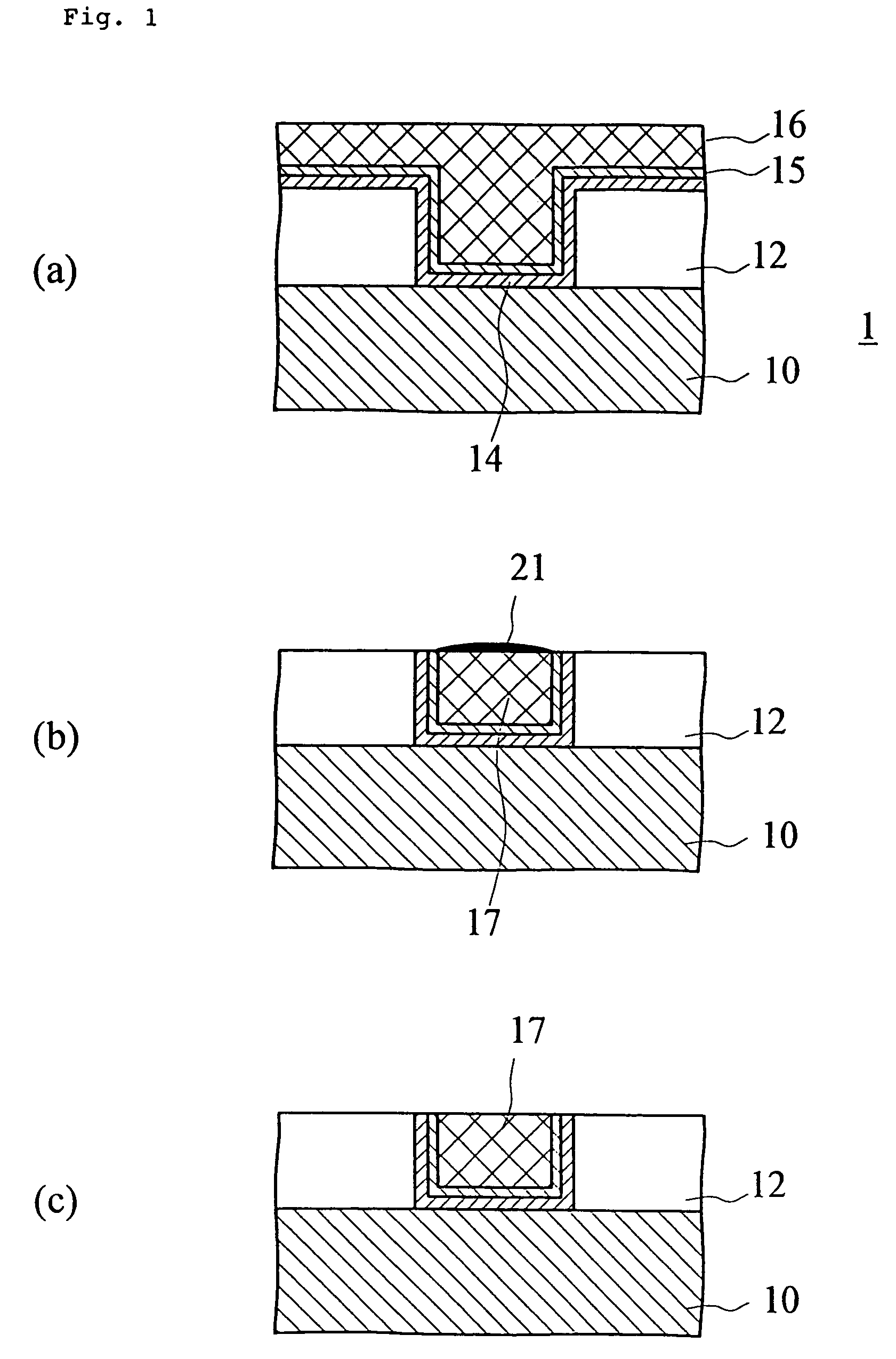
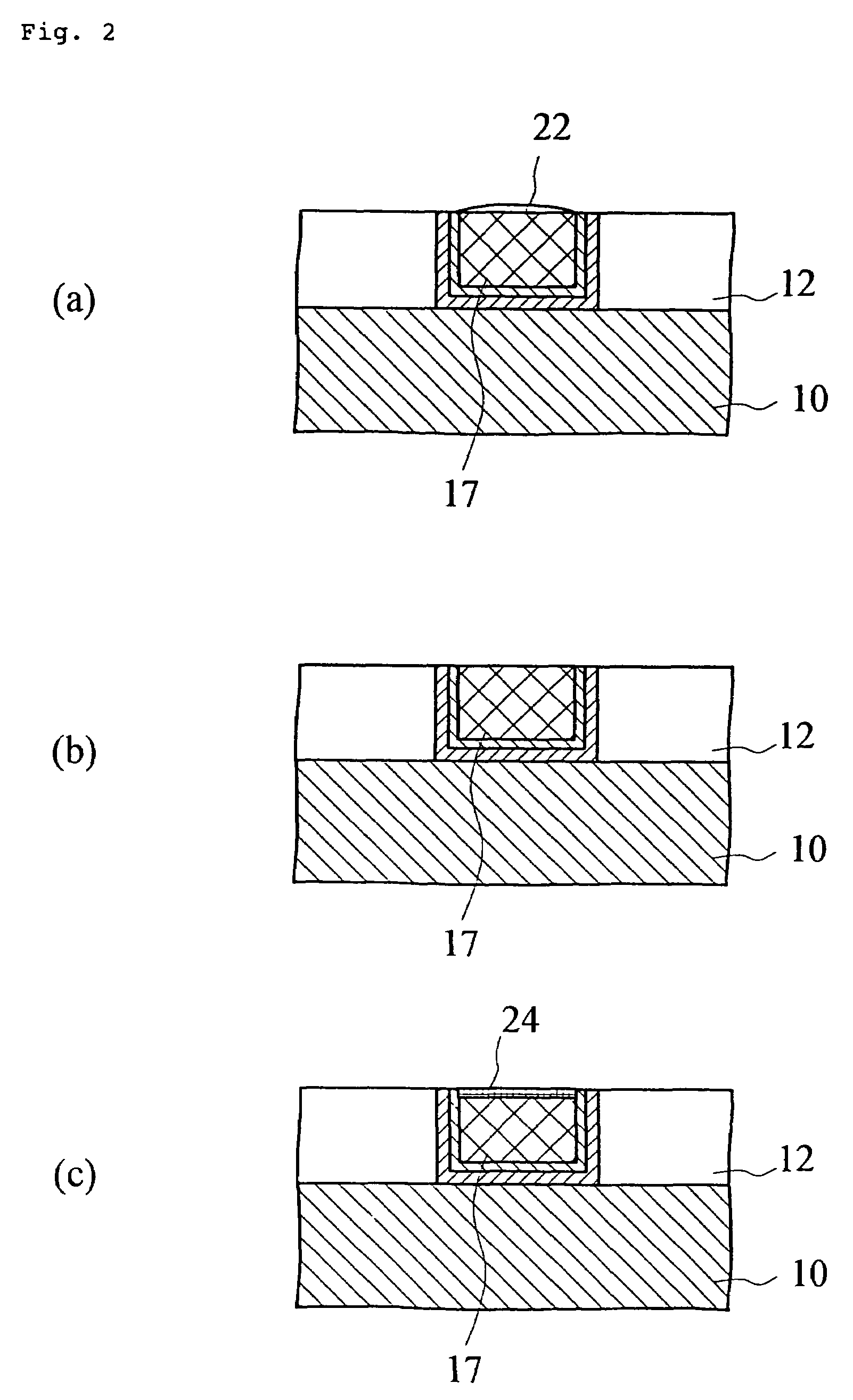
[0072]Using a method of manufacturing a semiconductor device according to the present invention, copper interconnections were formed and their interconnection lifetimes and resistances were evaluated. The method of fabricating the copper interconnection is described below. First, by the plasma CVD method, a silicon oxide film was formed on a silicon wafer. Next, by dry etching, a plurality of interconnection trenches patterned into a prescribed shape were formed. Next, after a barrier metal film was formed from Ta by the sputtering method, a seed copper film and a plating copper film were formed in this order.

[0073]Subsequently, the wafer surface was polished by the CMP method so as to leave copper inside of the interconnection trenches, and thereby a copper interconnection was formed. Next, for the purpose of removing polishing grains, particles such as polishing shavings, metals and slurries, which were adhered onto the surface of the semiconductor wafer, the following steps of cl...

case 2

for Comparison

[0080]Copper interconnections were formed in the same way as Example 1 except that, after the oxalic acid treatment, not an ammonia plasma treatment but only a BTA treatment was performed and thereafter a silicon nitride film was formed.

[0081]The copper interconnections fabricated as described in Example 1 and Cases 1 and 2 for Comparison have planar structures shown in FIGS. 6(a) and (b). The interconnection resistances and the interconnection life times for these copper interconnections were evaluated. With respect to the interconnection resistance, the evaluation was made through the value of resistance (E1 / I1) which was obtained by making an electric current (I1) flow between terminals for measurement P3-P4 of FIG. 6(a), while increasing from 0 A to 1 mA, and measuring the potential difference (E1) generated thereat between both ends P1-P2 of the measuring element. Regarding the interconnection lifetime, the evaluation was made through the measurement of the time p...

case 1

for Reference

[0083]On a silicon wafer, a silicon oxide film is formed and thereon a copper plating film is formed over the entire surface. Following that, after the copper surface was polished by the CMP method, for the purpose of removing polishing grains, particles such as polishing shavings, metals and slurries, the following steps of cleaning were performed.

[0084]First, a scrub cleaning was made. That is, particle contaminations were removed by moving a rotating brush, while spraying a cleaning agent made of electrolytic ionized water onto the brush. Next, a spin cleaning was made. In this step, while rotating the semiconductor wafer, a cleaning agent made of an aqueous solution containing 0.03 wt. % of oxalic acid was sprayed thereto for 10 seconds to remove metal contaminations which are CuO lying on the surface, and then rinsing with pure water was carried out.

[0085]Next, an anticorrosive treatment was made. The agent for the anticorrosive treatment used herein had the follow...


PUM

PropertyMeasurementUnit
Electrical resistanceaaaaaaaaaa

Abstract

In order to provide a manufacturing method of a semiconductor device which can improve the interconnection lifetime, while controlling the increase in resistance thereof, and, in addition, can raise the manufacturing stability; by applying a plasma treatment to the surface of a copper interconnection 17 with a source gas comprising a nitrogen element being used, a copper nitride layer 24 is formed, and thereafter a silicon nitride film 18 is formed. Hereat, under the copper nitride layer 24, a thin copper silicide layer 25 is formed.

Description

[0001]This is a divisional of application Ser. No. 10 / 071,184 filed Feb. 11, 2002 now U.S. Pat. No. 6,787,480.BACKGROUND OF THE INVENTION[0002]The present invention relates to a manufacturing method of a semiconductor device which comprises the steps of forming a copper-containing film, and more particularly to a manufacturing method of a semiconductor device having an interconnection, an interconnection connecting plug, a pad section or such, made of copper or a copper alloy.[0003]In recent years, copper and copper alloys have been widely used as the material for interconnections and connecting plugs to achieve higher speed operations in the elements with these metals utilized, the interconnections and the likes are generally formed by the damascene method.[0004]FIG. 5 is a series of views illustrating the steps of a conventional method of forming a copper interconnection. Now, this method is described below. First, as shown in FIG. 5(a), after an insulating film 10 and an interlay...

Claims


Application Information

Patent Timeline
IPC IPC(8): H01L21/324C23C8/48H01L21/02H01L21/304H01L21/308H01L21/314H01L21/316H01L21/318H01L21/3205H01L21/321H01L21/768H01L23/52
CPCH01L21/02074H01L21/0217H01L21/02211H01L21/02274H01L21/3143H01L21/3144H01L21/3148H01L21/31633H01L21/3185H01L21/321H01L21/3212H01L21/76802H01L21/76834H01L21/7684H01L21/76846H01L21/76849H01L21/76864H01L21/76867H01L21/76883H01L21/768
Inventor AOKI, HIDEMITSUTOMIMORI, HIROAKIOKADA, NORIOUSAMI, TATSUYAOHTO, KOICHITANIKUNI, TAKAMASA
Owner RENESAS ELECTRONICS CORP
Why Eureka
Try Eureka