Method and apparatus for improving performance margin in logic paths

a logic path and performance margin technology, applied in the field of logic on semiconductor chips, can solve the problems of path delay, path delay, and delay of individual logic blocks, and achieve the effects of less delay, high low voltage limit, and reliable operation

Inactive Publication Date: 2008-01-08
GOOGLE LLC
View PDF7 Cites 11 Cited by
  • Summary
  • Abstract
  • Description
  • Claims
  • Application Information

AI Technical Summary

Benefits of technology

[0010]The current invention teaches methods and apparatus to improve delay margins of logic paths on a semiconductor chip by dynamically controlling a supply voltage value to be as high as possible within a voltage range for the chip and without causing the chip to operate at a temperature in excess of a limit temperature chosen by a designer.
[0011]In an exemplary embodiment, a regulated unit comprises a semiconductor chip and a voltage regulator. A voltage controller on the semiconductor chip generates a control signal which is coupled to the voltage regulator. The voltage regulator supplies a voltage value to the semiconductor chip responsive to the control signal. The voltage controller dynamically adjusts the control signal to cause the voltage regulator to reduce the voltage value if a thermal sensor coupled to the voltage controller detects that a temperature on the semiconductor chip has exceeded a limit temperature, the limit temperature specified by a designer. The voltage controller dynamically adjusts the control signal to cause the voltage regulator to increase the voltage value if, after a predetermined time interval elapses, the thermal sensor has not detected that the temperature on the semiconductor chip has exceeded the limit temperature. The designer will specify voltage range having a high limit voltage and a low limit voltage. Sometimes, the low limit voltage is determined by performance characteristics of a particular chip; e.g., if the particular chip is known to be “slow” based on performance screen ring oscillator testing, that particular chip may have a slightly higher low voltage limit than a “fast” chip in order to operate reliably at a particular frequency. The high limit voltage is advantageously chosen to be at or near a maximum allowable voltage above which degradation or damage to the chip would occur. However, any suitable choices for the high limit voltage and the low limit voltage are contemplated. Typical logic paths on semiconductor chips, in particular, CMOS (Complementary Metal Oxide Semiconductor), have less delay at a higher supply voltage than at a lower supply voltage. Therefore, operating the chip at as high a voltage as possible within the voltage range specified for the chip, without exceeding the limit temperature, reduces logic path delays and improves a timing margin on the semiconductor chip.

Problems solved by technology

Process variations, such as FET (field effect transistor) channel length are a major contributor to delays of individual logic blocks, such as NANDs and NORs, which contribute to delays of logic paths.
Carrier mobility, interconnection wiring, implant doping, and many other characteristics of the FETs and interconnect all have process variations that affect delay of individual logic blocks, and, ultimately, path delays.
External conditions also affect delays of individual logic blocks and path delays.
Typically, CMOS circuits become slower, that is, have longer delays, as temperature increases.
Supply voltage has a major effect on delays.
In older, lower performance CMOS processes, static power was very low, and often negligible.
Gate oxide thicknesses have become only a few atomic layers thick; leakage through such a thin FET gate oxide to underlying regions results in a significant fraction of a total power dissipated by the chip.

Method used


Image

  • Method and apparatus for improving performance margin in logic paths
  • Method and apparatus for improving performance margin in logic paths
  • Method and apparatus for improving performance margin in logic paths

Examples


second embodiment

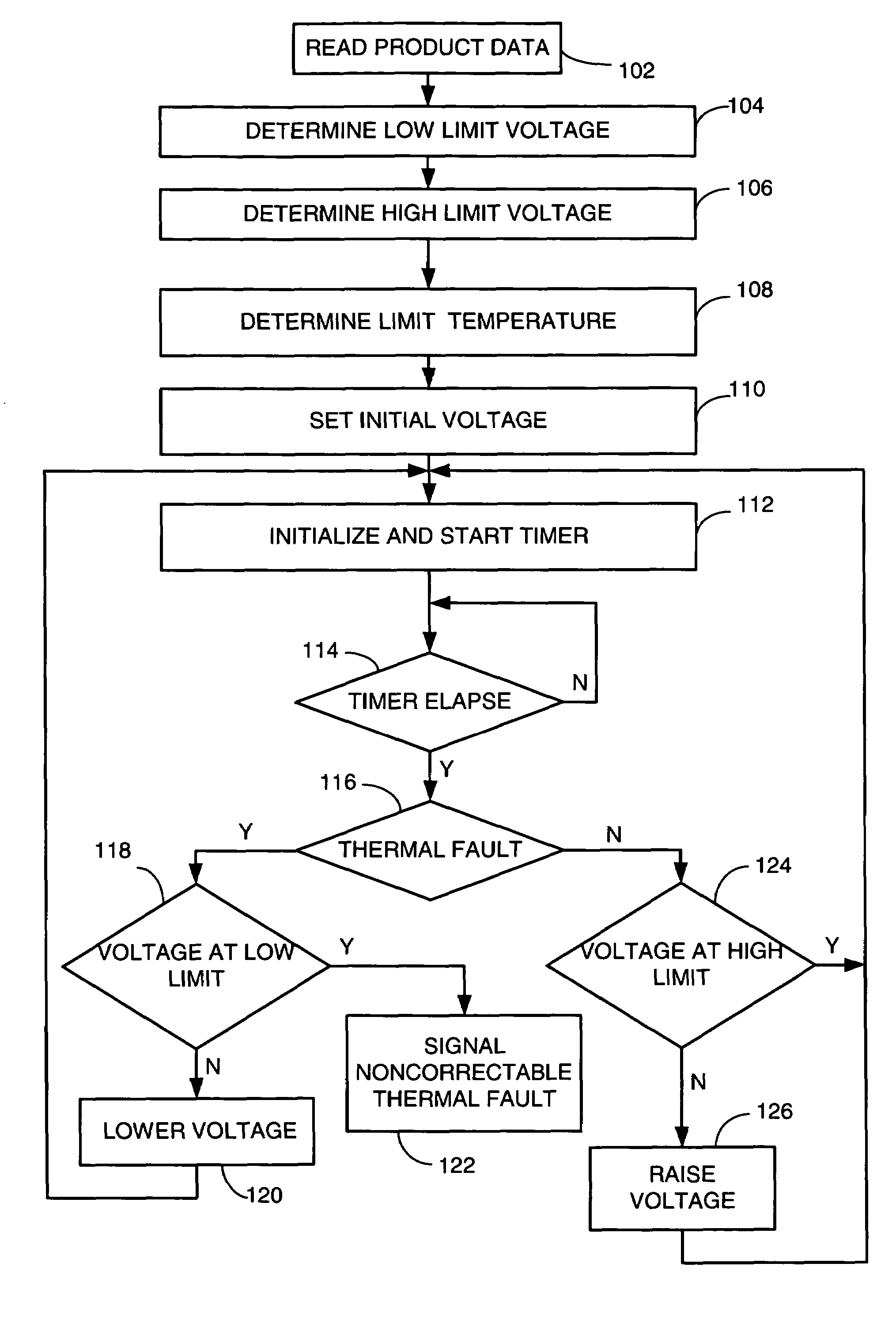
[0040]Voltage controller 22 is coupled to a product data 24 using coupling 72, product data 24 constructed of storage on chip 21. Product data 24 stores chip information about chip 21 that is needed by voltage controller 22 to determine what logical values to drive on VID 28 to cause voltage regulator 26 to produce a voltage value on VDD 27 that improves a timing margin on a path on chip 21. Examples of chip information stored in product data 24 include, but are not limited to, limit temperature, high limit voltage, low limit voltage, timer initialization value or values, thermal data used by voltage controller 22 to determine a rate at which to change voltage; and thermal time constant information. In an embodiment, product data 24 is implemented in nonvolatile storage such as a fuse arrangement, a flash memory, an EEPROM (electrically erasable programmable read only memory), FERAM (ferroelectric random access memory), or other suitable nonvolatile storage. In a second embodiment, ...

first embodiment

[0041]Voltage controller 22 is coupled to a timer 25 by couplings 74 and 75. Timer 25 is designed to be initialized, started, and to report to voltage controller 22 on coupling 74 upon elapse of a predetermined time interval. In a first embodiment, the timer is reset, or initialized, by voltage controller 22, using coupling 75, to a fixed value and counts to a second value that indicates the elapse of the predetermined time interval. For example, timer 25 may be a simple 16-bit counter that is initialized to “0”. When timer 25 is started, it counts upward until the counter overflows; the overflow indicating that the predetermined interval (i.e., how long it takes to overflow a 16 bit counter at a particular clock frequency) has elapsed. Alternatively, timer 25 may be a 16-bit counter initialized to “1” but configured to count down, with the elapse of the predetermined time interval occurring when the counter is “0”. In a more general case, timer 25 is programmable, allowing a first ...


PUM


Abstract

An apparatus and method is disclosed for improving timing margins of logic paths on a semiconductor chip. Typical logic embodiments, such as CMOS (Complementary Metal Oxide Semiconductor), have path delays that become shorter as supply voltage is increased. Embodiments of the present invention store product data on each particular chip. The product data includes, for examples, but not limited to, a voltage range having a low limit voltage and a high limit voltage, a limit temperature, and performance of the particular chip in storage for the particular chip. Each chip has a voltage controller, a timer, and a thermal monitor. The voltage controller communicates with a voltage regulator and dynamically causes a voltage supply coupled to the chip to be as high as possible in the voltage range, subject to the limit temperature.

Description

BACKGROUND OF THE INVENTION[0001]1. Field of the Invention[0002]The current invention generally relates to logic on semiconductor chips. More specifically the current invention is directed to increasing performance margin of logic paths on the chips, consistent with environmental conditions.[0003]2. Description of the Related Art[0004]Semiconductor chips comprising logic circuits arranged in logic paths that perform useful functions are well known. For example, modern computer processors are built with one or more semiconductor chips with logic circuits arranged in such a way as to perform addition, shifting, rotating, comparing and many other functions needed to perform the operation of the computer processor. Storage used by the modern computer processors comprise dynamic random access memory (DRAM) and static random access memory (SRAM) that are also built on semiconductor chips.[0005]Complementary Metal Oxide Semiconductor (CMOS) logic circuitry is the predominant semiconductor ...

Claims


Application Information

Patent Timeline
Patent Type & Authority Patents(United States)
IPC IPC(8): H02H5/04G11C7/00
CPCG06F1/206G06F1/26G11C5/147G11C7/04G11C11/4074
Inventor DONZE, RICHARD LEEHOVIS, WILLIAM PAULKUEPER, TERRANCE WAYNESHEETS, II, JOHN EDWARDTETZLOFF, JON ROBERT
Owner GOOGLE LLC
Why Eureka
Try Eureka