Method of epitaxial-like wafer bonding at low temperature and bonded structure

a technology of epitaxial-like wafers and low temperature, applied in the direction of electrical equipment, semiconductor devices, semiconductor/solid-state device details, etc., can solve the problems of large density of threading dislocations in the bulk of the layers, severe and often damaging thermal stresses, and unwanted changes in the bonding material

Inactive Publication Date: 2008-02-19
INVENSAS BONDING TECH INC
View PDF166 Cites 28 Cited by
  • Summary
  • Abstract
  • Description
  • Claims
  • Application Information

AI Technical Summary

Problems solved by technology

Conventional hetero-epitaxial growth techniques applied to these lattice mismatched active layers usually result in a large density of threading dislocations in the bulk of the layers.
To bond wafers composed of thermally mismatched materials, severe and often damaging thermal stresses can be induced with high temperature annealing.
The high temperature annealing process can also produce unwanted changes to bonding materials and often prevents the bonding of processed device wafers.
The bonding materials may decompose at high temperatures, even if the bonding wafers are thermally matched.
The bonding energy of conventional HF dipped hydrophobic silicon wafer pairs is higher than the hydrogen-induced region only after annealing at temperatures higher than 600° C. Therefore, this process does not work for oxide-free hydrophobic silicon wafer bonding.
Therefore, the smart-cut method for a layer transfer using conventional HF-dipped silicon wafer pairs is not possible because the bonding energy is too low at layer transfer temperatures that are lower than 500° C.

Method used


Image

  • Method of epitaxial-like wafer bonding at low temperature and bonded structure
  • Method of epitaxial-like wafer bonding at low temperature and bonded structure
  • Method of epitaxial-like wafer bonding at low temperature and bonded structure

Examples


example

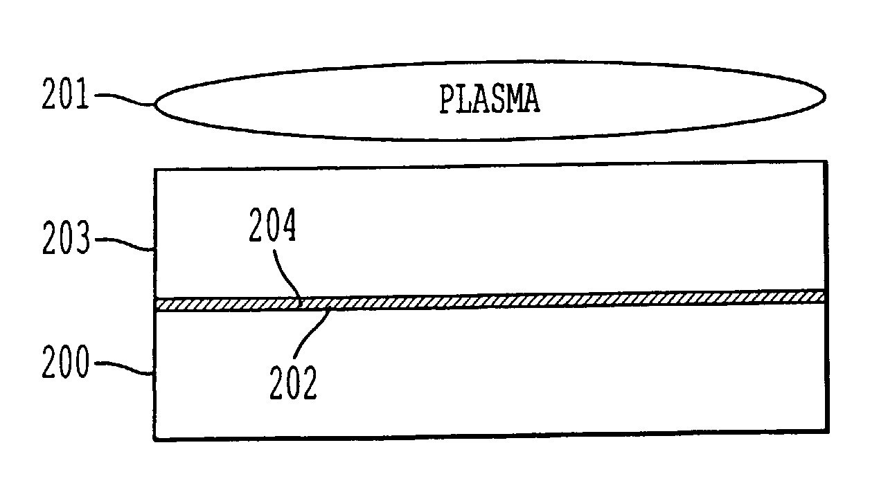
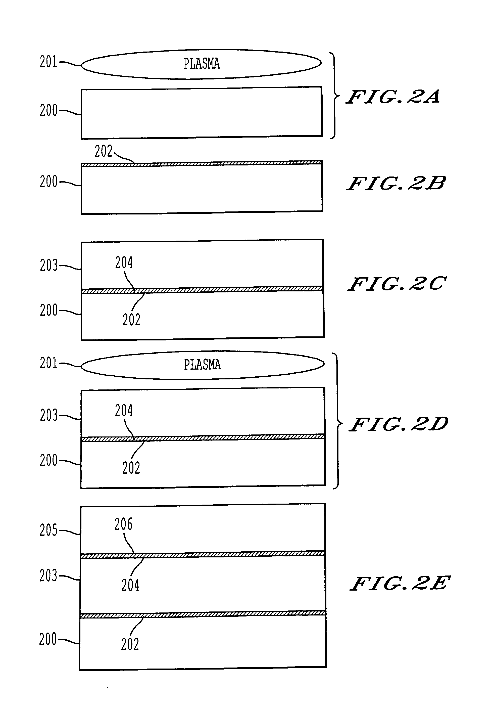
[0056]75 mm diameter, 1-10 ohm-cm, p-type Si (100) substrate wafers were used. The wafers were cleaned in a RCA-1 solution, dipped in a 1% hydrofluoric aqueous solution followed by treatment in B2H6 plasma for an appropriate time period depending on the plasma system used. Appropriate plasma treatment times have ranged from 30 sec. to 5 min. The B2H6 plasma treatment consisted of a mixed gas of 20 sccm of 0.5% B2H6 / 99.5% He and 20 sccm Ar in an inductor coupled plasma (ICP) operating in a reactive ion etch mode with a RF power of 38 W at a pressure of ˜5 mTorr. A ˜100 V self-biased voltage was generated. This self-bias is the lowest possible self-bias for a stable plasma treatment in the plasma treatment system used herein. The wafers were then dipped in a diluted 1% HF solution to remove any oxide on the wafer surfaces. The wafers were then placed together without water rinse and bonded in air at room temperature.

[0057]The bonded wafer pair was stored in a low vacuum chamber at a v...


PUM


Abstract

A process for bonding oxide-free silicon substrate pairs and other substrates at low temperature. This process involves modifying the surface of the silicon wafers to create defect regions, for example by plasma-treating the surface to be bonded with a or boron-containing plasmas such as a B2H6 plasma. The surface defect regions may also be created by ion implantation, preferably using boron. The surfaces may also be amorphized. The treated surfaces are placed together, thus forming an attached pair at room temperature in ambient air. The bonding energy reaches approximately 400 mJ / m2 at room temperature, 900 mJ / m2 at 150° C., and 1800 mJ / m2 at 250° C. The bulk silicon fracture energy of 2500 mJ / m2 was achieved after annealing at 350-400° C. The release of hydrogen from B—H complexes and the subsequent absorption of the hydrogen by the plasma induced modified layers on the bonding surfaces at low temperature is most likely responsible for the enhanced bonding energy.

Description

BACKGROUND OF THE INVENTION[0001]1. Field of the Invention[0002]The present invention relates to a method of epitaxial-like bonding of wafer pairs at low temperature, and more particularly to a method of bonding in which the wafer surfaces are modified to create surface and subsurface defect areas, and possibly amorphized, by ion implantation or plasma, preferably by boron-containing ions or a plasma such as B2H6.[0003]2. Discussion of the Background[0004]For many optoelectronic and electronic device applications, homo-epitaxial single crystalline layers consisting of same material with same crystalline orientation but different doping types or levels are necessary. For some device applications, active layers comprising single crystalline dissimilar materials are required. The active layers should be high crystallographic quality with interfaces that are thermally conductive and almost optical loss free. Conventional hetero-epitaxial growth techniques applied to these lattice mismat...

Claims


Application Information

Patent Timeline
Patent Type & Authority Patents(United States)
IPC IPC(8): H01L21/48H01L21/18H01L21/302H01L21/306
CPCH01L21/02052H01L21/187H01L21/306Y10S438/974
Inventor TONG, QIN-YI
Owner INVENSAS BONDING TECH INC
Why Eureka
Try Eureka