Method for processing semiconductor wafer and semiconductor wafer

a technology of semiconductor wafers and processing methods, applied in the field of semiconductor wafers, can solve the problems of reducing the flatness of the wafer in proportion to the increase of the etching removal, the damage of the etching, so as to achieve the effect of less mechanical damage, easy production and high flatness

Inactive Publication Date: 2008-02-19
SHIN-ETSU HANDOTAI CO LTD
View PDF20 Cites 10 Cited by
  • Summary
  • Abstract
  • Description
  • Claims
  • Application Information

AI Technical Summary

Benefits of technology

[0098]TABLE 3Qualities of waferPWBack surfaceKinds of etchantFlatnessWavinessstock removalconditionAlkaline solution⊚⊚ (Small)X (Large)X (Rough)(NOH or KOH)(Good)Acid solutionX (Bad)X (Big)◯ (Small)⊚ (Smooth)(Acetic acid type)Combination◯◯ΔΔ(Alkaline + Acetic acid type)Present invention◯⊚⊚◯(Alkaline + Phosphoric acid type)[Note]Acetic acid type (Hydrofluoric acid + Nitric acid + Acetic acid),Phosphoric acid type (Hydrofluoric acid + Nitric acid + Phosphoric acid)
[0099]In this regard, if an etching removal (stock removal by etching) is too large, peripheral sags on a wafer are easily generated even by an etching of alkaline etching and acid etching. Therefore, in the etching process, it is preferable that the etching amount is set at about 10-30 μm on both sides in total that is smaller than a conventional stock removal. Preferably, it is set at 15 μm on both sides in total for alkaline etching and about 5 μm on both sides in total for acid etching.
[0100]According to the above-described two-stage chemical etching of alkaline etching+phosphoric acid type mixed acid etching of the present invention, a semiconductor wafer having the maximum value of pit depth of 4 μm or less, PV value of 0.05 μm or less of which waviness is at a pitch of 2 mm, and glossiness range of 20-70% can be easily produced stably.
[0101]The present inventors also performed various studies on a method for producing a wafer having less mechanical damages, pits generated due to the damages or the like before a mirror-polishing process, particularly an etching process, and its previous process, and as the result, it was conceived that by incorporating a surface grinding process as substitute for a lapping process or after a lapping process, a damaged layer generated due to slicing or lapping is extremely reduced, and a wafer maintaining a high flatness is obtained, and moreover, the wafer is subjected to alkaline etching to remove a damaged layer and grinding striation remaining in the surface grinding, and in order to improve pits due to remaining grinding striation, acid etching is performed with a mixed aqueous solution composed of hydrofluoric acid, nitric acid and phosphoric acid as an acid etchant, and the present invention was completed through investigations of processing conditions.
[0102]FIG. 1 includes series of flowcharts of processing a single crystal ingot to produce a semiconductor mirror-polished wafer. FIG. 1(a) is a flowchart showing a surface grinding process and an etching process in order. FIG. 1(b) is a flowchart showing a surface grinding process that a lapping process is added in front of the surface grinding process, and an etching process in order.
[0103]FIG. 1(a) shows a process for producing a mirror-polished wafer that a lapping process is completely substituted with a surface grinding process. A wafer is obtained by slicing a single crystal ingot in a slicing process, and the wafer is subjected to surface-grinding in a surface grinding process to improve its flatness and to remove a mechanical damaged layer generated in the slicing process. Next, the wafer is subjected to chamfering processing in a chamfering process, and the process enters upon an etching process. In the etching, alkaline etching is firstly performed to remove or shallow a damaged layer and a grinding striation, and then acid etching is performed with phosphoric acid type mixed acid to make a grinding striation shallow. On the occasion, it is preferable that an etching removal of the alkaline etching is larger than that of the acid etching. Subsequently, mirror polishing is performed in a mirror-polishing process, and cleaning and drying are performed in a cleaning / drying process to manufacture a mirror-polished wafer having high flatness.

Problems solved by technology

By acid etching, a mechanically damaged layer can be removed, but flatness of a wafer is easily degraded in proportion to increase of its etching removal.
Also, there is a problem that harmful NOX is generated by chemical reaction in acid etching.
However, by increasing stock removals, the flatness is degraded by polishing and productivity of a polishing process is decreased drastically.
As a result, although the flatness was able to be achieved sufficiently, it was not always enough reduction of a stock removal to obtain a mirror-polished wafer (PW).
However, it was difficult to control a residual grinding striation and a grinding damage by grinding, and it was difficult to control a grinding damage at 3 μm or less.
Conventionally, sometimes mirror-polishing has been performed on both sides of a wafer, but if a back surface thereof is completely mirror-polished (its glossiness is increased around 100%), there is a problem that particles are easily attached thereto and easily released therefrom again, or a problem of a contact area such as a electrostatic chuck or the like used for adsorbing a wafer, so that it is necessary to decrease glossiness to a certain range.
According to this, glossiness can be controlled to about 40%, but sometimes there is a problem that when an etching amount was further reduced, glossiness was reduced to 20% or less.
Therefore, in the case that a method for processing a semiconductor wafer that acid etching is performed after alkaline etching, there was a problem of quality of a back surface thereof.

Method used


Image

  • Method for processing semiconductor wafer and semiconductor wafer
  • Method for processing semiconductor wafer and semiconductor wafer
  • Method for processing semiconductor wafer and semiconductor wafer

Examples


example 1

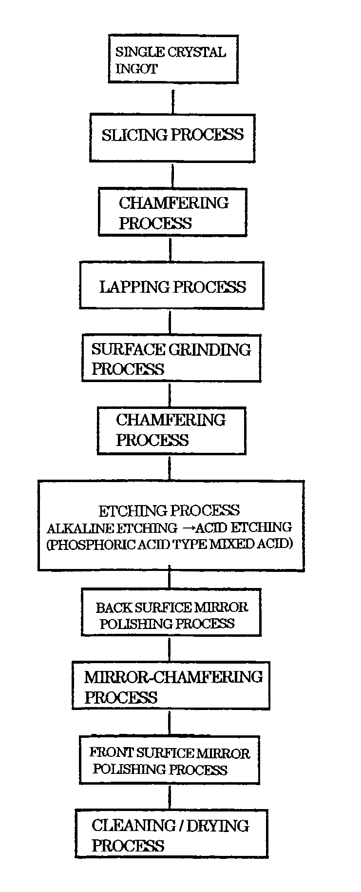
[0131]As the result of the above consideration, in view of the pit depth, the surface condition, the etching rate, and the stability of the etchant, it was found that an etchant of which mixing ratio is hydrofluoric acid of 50% by weight:nitric acid of 70% by weight:phosphoric acid of 85% by weight=1:3:2, that is, an etchant of HF=6.6% by weight, HNO3=34.0% by weight, H3PO4=32.5% by weight, the retained material of H2O (26.9% by weight), and the meltage of silicon=19 g / L, was preferable. The following is the explanation of examples using this acid etchant.

[0132]The following etching treatment was performed for lapped wafers (lapping abrasive grain size: #1200) having a diameter of 200 mm (8 inches). TTV of this lapped wafer was about 0.8 μm.

[0133]First, the wafers were immersed in an NaOH aqueous solution having a concentration of 50% by weight at 85° C. for 450 seconds in order to perform alkali etching with a target etching amount being set to 20 μm on both sides in total. Subsequ...

example 2

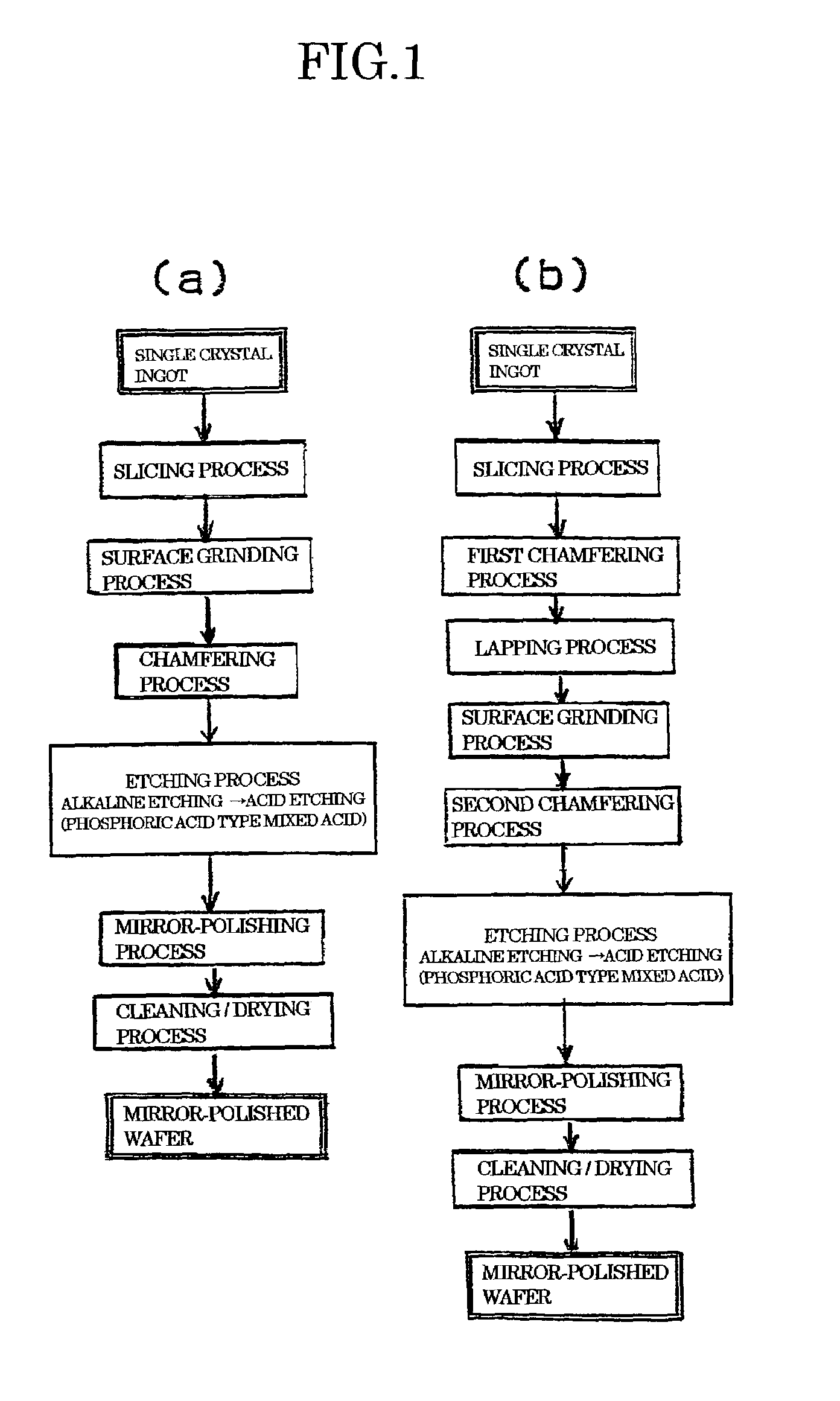
[0147]Mirror-polished wafers were produced in the process as shown in FIG. 1(b), the wafers were prepared by slicing an ingot having a diameter of about 200 mm, the sliced wafers were subjected to first chamfering, then the wafers were lapped by using a lap slurry (lapping abrasive grain size: #1200), and by using the wafer (called lapped wafer), surface grinding was performed on the following conditions.

[0148]Surface grinding was performed by using an in-feed type single-side grinding apparatus, a spindle rotational speed was 5500 rpm, a wafer rotational speed was 7 rpm, and the feed rate of a grinding stone was 0.2 μm / sec. Then after, second chamfering was performed.

[0149]After this surface grinding, flatness (TTV) of the wafer was about 0.6 μm.

[0150]Next, as to alkaline etching, the wafers were immersed in an NaOH aqueous solution having a concentration of 50% by weight at 85° C. for 450 seconds in order to perform alkali etching with a target etching amount being set to 20 μm on...

example 3

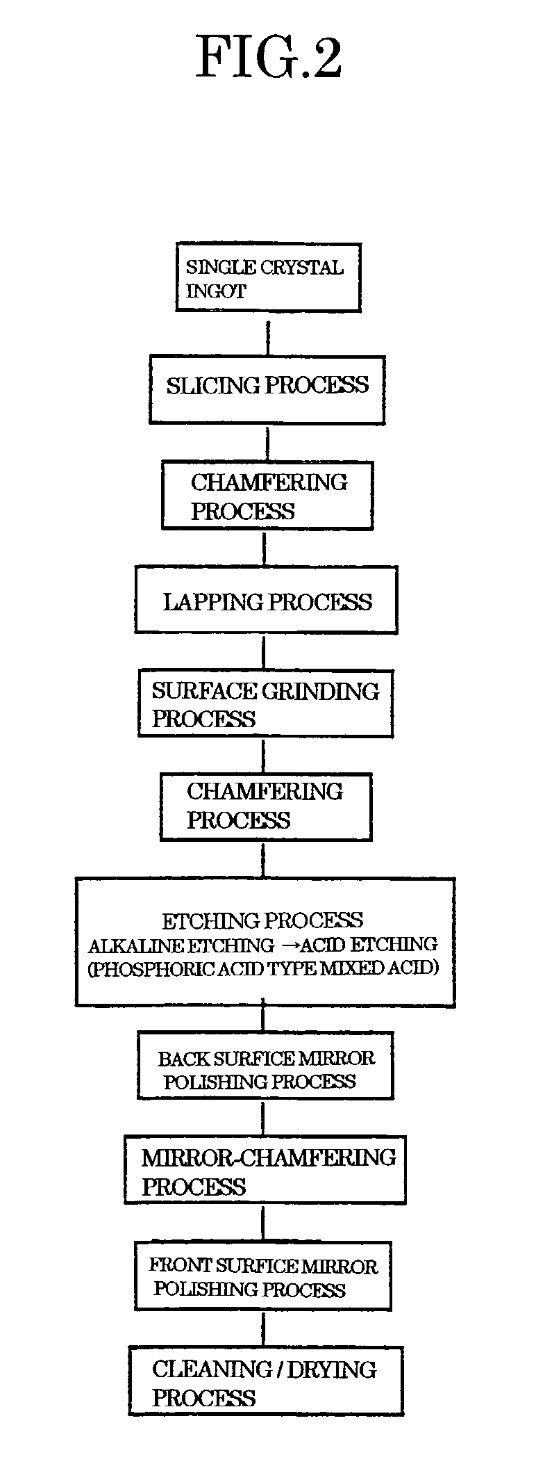
[0173]Mirror-polished wafers were produced by the process as shown in FIG. 2. The wafers were obtained by slicing a single crystal rod (ingot) having a diameter of 200 mm and resistivity of 0.02 Ù·cm with a wire saw, and after a first chamfering, the wafers were subjected to lapping of 40 μm on both sides in total by using lapping slurry (lapping abrasive grain size: #1200). Next, replacing the above lapping slurry with lapping slurry of lapping abrasive grain size of #1500, the wafers were further subjected to lapping of 20 μm on both sides in total.

[0174]Subsequently, surface grinding was performed. The surface grinding was performed by using an in-feed type single-side grinding apparatus and using a grinding stone of #4000 at 10 μm on a single side of the wafers. The conditions of the surface grinding were that a spindle rotational speed was 5500 rpm, a wafer rotational speed was 7 rpm, and the feed rate of the grinding stone was 0.2 μm / sec. Then after, a second chamfering was pe...


PUM

PropertyMeasurementUnit
concentrationaaaaaaaaaa
surface roughnessaaaaaaaaaa
thicknessaaaaaaaaaa

Abstract

There is provided a method for processing a semiconductor wafer subjected to a chamfering process, a lapping process, an etching process, and a mirror-polishing process, wherein acid etching is performed after alkaline etching as the etching process, and the acid etching is performed with an acid etchant composed of hydrofluoric acid, nitric acid, phosphoric acid, and water, a method for processing a semiconductor wafer subjected to a chamfering process, a surface grinding process, an etching process, and a mirror-polishing process, wherein the etching process is performed as described above, and a method for processing a semiconductor wafer subjected to a flattening process, an etching process, and a mirror-polishing process, wherein the etching process is performed as described above, a back surface polishing process is performed after the acid etching as the mirror-polishing process, and then a front surface polishing process is performed. According to this, there can be provided a method for processing a semiconductor wafer to have good flatness, good surface roughness, and good condition on a back surface thereof.

Description

TECHNICAL FIELD[0001]The present invention relates to a semiconductor wafer and more particularly relates to the improvement of a method to remove a mechanically damaged layer on a wafer surface generating in a production process of the single crystal silicon wafer by a chemical etching and the improvement of a wafer back surface state resulted from a production method of the single crystal silicon wafer.BACKGROUND ART[0002]Conventionally, a production process of semiconductor mirror-polished wafers usually comprises processes that wafers are obtained by slicing a single crystal ingot made of silicon or the like, and the obtained semiconductor wafers are subjected to at least chamfering, lapping, etching, mirror-polishing, and cleaning / drying. An example of such a production process of semiconductor mirror-polished wafers is shown in FIG. 3. These processes are performed variously depending on the purpose, that is, a part of the process is replaced or repeated plural times, or proce...

Claims


Application Information

Patent Timeline
Patent Type & Authority Patents(United States)
IPC IPC(8): H01L21/461H01L21/304H01L21/306
CPCH01L21/02008H01L21/30604H01L21/306
Inventor NIHONMATSU, TAKASHIYOSHIDA, MASAHIKOSASAKI, YOSHINORISAITOH, MASAHITOTAKAKU, TOSHIAKIKATO, TADAHIRO
Owner SHIN-ETSU HANDOTAI CO LTD
Why Eureka
Try Eureka