Process for producing SOI wafer

a silicononinsulator and soi technology, applied in the direction of basic electric elements, electrical apparatus, semiconductor devices, etc., can solve the problems of uneven polishing layer amount, difficult to obtain uniform film thickness distribution in the soi layer, and etching irregularities tend to occur

Active Publication Date: 2008-04-15
SUMCO CORP
View PDF13 Cites 4 Cited by
  • Summary
  • Abstract
  • Description
  • Claims
  • Application Information

AI Technical Summary

Benefits of technology

[0010]It is a further object of this invention to provide a process for producing an SOI wafer that provides a uniform film thickness for the SOI layer while making the SOI layer extremely thin.
[0012]In this process for producing an SOI wafer, an ion implantation layer is formed on a wafer that is used for the active layer using a process for forming an SOI wafer that is based on a Smart Cut method. Next, this active layer wafer is bonded via an insulating film onto a base wafer. As a result, a bonded wafer is produced in which two wafers are bonded together via an insulating film. Subsequently, by performing cleaving heat processing on this bonded wafer, cleaving can be achieved taking the ion implantation layer as a boundary. At this time, the roughness (root mean square; rms) of the surface of the SOI wafer after cleaving is 10 nm or less.
[0015]As a result, the root mean square roughness (rms) (10 μm×10 μm) of the surface of the SOI wafer can be reduced to 0.1 nm or less.
[0017]In the heat processing of an SOI wafer that is based on a Smart Cut method, there is cleaving heat processing in which cleaving is performed using the ion implantation layer as a boundary, and enhancement bonding heat processing in which the bonding between the active layer wafer and the base wafer after the cleaving is enhanced. After the cleaving heat processing, the SOI wafer is damaged by the cleaving and the surface thereof has been roughened. Therefore, after the cleaving processing, smoothing heat processing is performed by holding the SOI wafer in an inert gas atmosphere at a predetermined temperature. Subsequently, oxidization processing is performed on the SOI wafer in the oxidizing atmosphere. This oxide film is removed using, for example, HF solution. As a result, the SOI layer can be made thinner.
[0020]In this process for producing an SOI wafer, the SOI wafer is heat processed by being held for approximately three hours at a temperature of 1100° C. or more. The argon gas has a smaller etching effect on the surface of the SOI wafer than does hydrogen gas. However, it does have the effect of making the surface of the SOI wafer that has become rough after the cleaving smooth as a result of the re-crystallization (i.e., of the migration). As a result, the surface of the SOI wafer is re-crystallized (i.e., migration occurs) and, in addition, the surface thereof is smoothed. If the temperature of the smoothing heat processing is 1100° C. or more, then the surface of the SOI wafer is sufficiently re-crystallized. Moreover, this heat processing can also perform the additional function of strengthening the adhesion.
[0028]As a result, according to the present invention, it is possible to reduce the root mean square roughness (rms) (10 μm×10μ) of the surface of this SOI layer to 0.1 nm or less.

Problems solved by technology

However, as a result of damage caused by the cleaving, the surface of the SOI wafer after the cleaving (i.e., the cleaving surface) ends up as a rough surface.
However, in the mechanical processing method described in Patent Document 1, the amount of polishing layer is non-uniform, and it is difficult to obtain a uniform film thickness distribution in the SOI layer.
However, in the method of manufacturing an SOI wafer described in Patent Document 2, if smoothing processing is performed using a hydrogen gas etching effect, then etching irregularities tend to occur.
These etching irregularities cause the film thickness of the SOI layer to not be uniform.
Moreover, because safety devices are required due to the use of hydrogen gas, the resulting equipment costs are high which creates problems from a financial standpoint.

Method used


Image

  • Process for producing SOI wafer
  • Process for producing SOI wafer
  • Process for producing SOI wafer

Examples


Embodiment Construction

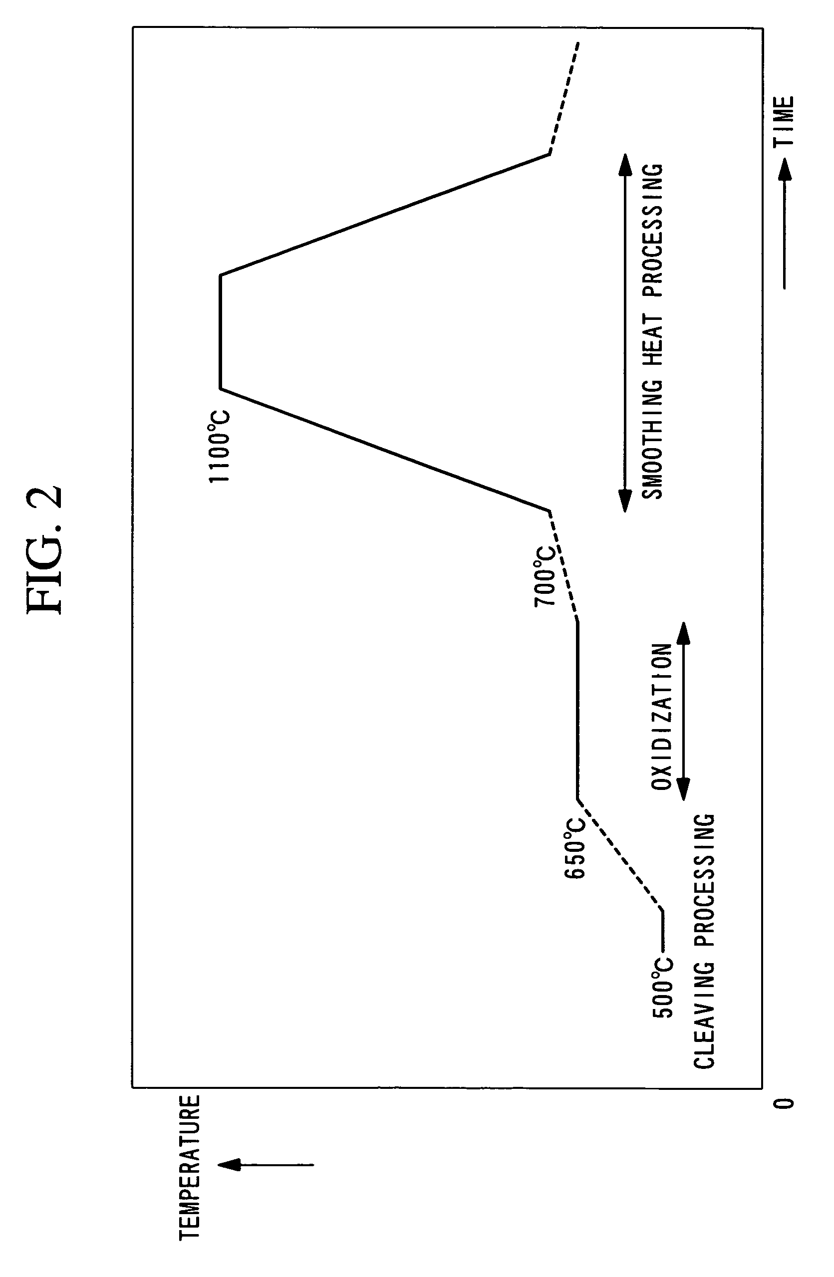
[0032]An embodiment of this invention will now be described with reference to FIGS. 1 and 2.

[0033]Here, a process for producing an SOI wafer in which an SOI layer is formed using a Smart Cut method is described.

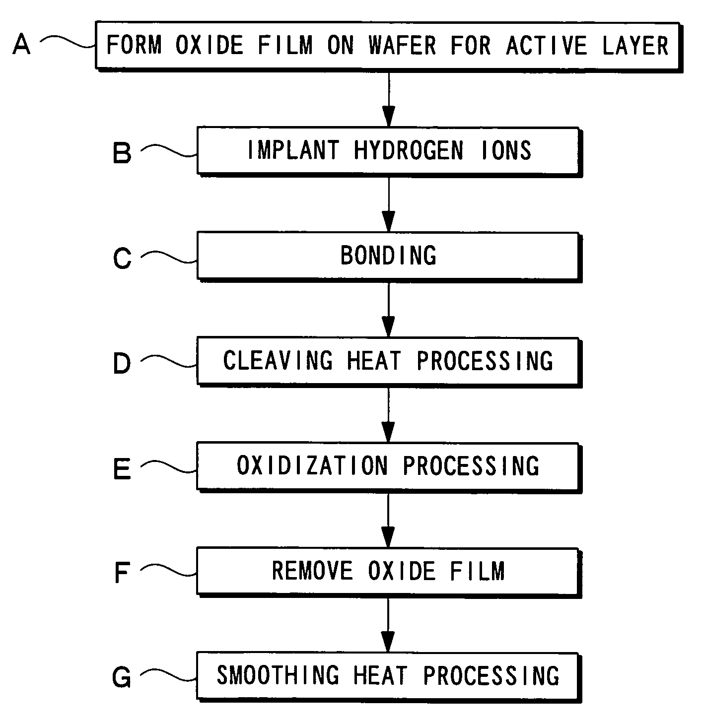
[0034]The production of an SOI wafer using a Smart Cut method according to the present embodiment is achieved using steps such as that shown in A to G in FIG. 1.

[0035]Firstly, two silicon wafers are prepared by taking slices from a silicon ingot that has been grown using a CZ method and doped with boron. One of these two silicon wafers is used for an active layer, while the other silicon wafer is used for base. Moreover, as is shown in step A in FIG. 1, an oxide film is formed on a surface of the silicon wafer that is used for the active layer. The oxide film is formed by placing the silicon wafer inside an oxidization furnace and then heating it at a predetermined temperature for a predetermined length of time. At this time, the thickness of the oxide film that is formed is ...


PUM


Abstract

There is provided a process for producing an SOI wafer in which, when producing an SOI wafer using Smart Cut technology, the surface can be smoothed after cleaving, the thickness of the SOI layer can be reduced, and the film thickness of the SOI wafer can be made uniform. In this process for producing an SOI wafer, hydrogen gas ions are implanted via an oxide film in a silicon wafer that is to be used for an active layer, so that an ion implanted layer is formed in the silicon bulk. Next, this active layer silicon wafer is bonded via an insulating film to a base wafer. By heating this base wafer, a portion thereof can be cleaved using the ion implanted layer as a boundary, thereby forming an SOI wafer. After the cleaving has been performed using the ion implanted layer as a boundary, the SOI wafer undergoes oxidization processing in an oxidizing atmosphere. This oxide film is then removed by, for example, HF solution. Thereafter, the SOI wafer undergoes heat processing for approximately three hours in an argon gas atmosphere at 1100° C. or more. As a result, the root mean square roughness of the SOI wafer surface is improved to 0.1 nm or less.

Description

TECHNICAL FIELD[0001]The present invention relates to a process for producing a silicon-on-insulator (SOI) wafer and specifically to a process for producing an SOI wafer in which the surface of the SOI wafer is smoothed.[0002]Priority is claimed on Japanese Patent Application No. 2004-3347, filed Jan. 8, 2004, the content of which is incorporated herein by reference.BACKGROUND ART[0003]Compared to conventional silicon wafers, SOI wafers are superior in that separation between elements, a reduction in parasitic capacitance between an element and a substrate, and a three-dimensional structure are all possible, and they are consequently used in high-speed, low power consumption LSI.[0004]One method for producing an SOI wafer is a Smart Cut method in which hydrogen ions are implanted in the silicon wafer surface and then cleaving heat processing is performed with the result that cleaving can be performed using the ion implantation layer as a boundary. However, as a result of damage caus...

Claims


Application Information

Patent Timeline
Patent Type & Authority Patents(United States)
IPC IPC(8): H01L21/76H01L21/02H01L27/12H01L21/302H01L21/762
CPCH01L21/302H01L21/76254
Inventor MORIMOTO, NOBUYUKINISHIHATA, HIDEKI
Owner SUMCO CORP
Why Eureka
Try Eureka