Substrate processing apparatus

a processing apparatus and substrate technology, applied in the direction of grinding drives, grinding machine components, manufacturing tools, etc., can solve the problems of b> type of irregularities, > difficult to control, and difficult to remove surface roughness, so as to achieve the effect of removing surface roughness

Inactive Publication Date: 2008-05-06
EBARA CORP +1
View PDF18 Cites 54 Cited by
  • Summary
  • Abstract
  • Description
  • Claims
  • Application Information

AI Technical Summary

Benefits of technology

[0015]The present invention has been made in view of the above drawbacks in the prior art, and it is, therefore, an object of the present invention to provide a substrate processing apparatus which can effectively remove surface roughness produced at a peripheral portion of a substrate or the like or a film attached to a peripheral portion of a substrate or the like, which would cause contamination, in a manufacturing process of a semiconductor device or the like.

Problems solved by technology

One of the major problems in managing particles is dust caused by surface roughness produced at a bevel portion and an edge portion of a semiconductor wafer (substrate) in a manufacturing process of semiconductor devices.
These types of irregularities 550 may be problematic because dust tends to accumulate in the irregularities 550 during subsequent processes such as CMP (Chemical Mechanical Polishing).
However, the conventional CDE method has difficulty in completely removing such surface roughness at the bevel portion and the edge portion of the Si wafer 100.
Further, the time required for processing a single wafer in a CDE process is usually 5 minutes or more, and hence a CDE process has problems in that it causes a lower throughput and has high material costs.
Particularly, in a manufacturing process of a semiconductor device, since films of new materials which are attached to a bevel portion, an edge, and a reverse face of a wafer may cause contamination, removal of such films represents an important problem.
With the CVD method, attachment of a Ru film to a bevel portion, an edge portion, and a reverse face is unavoidable, while degrees of the attachment are different depending on device arrangements.
Even if a Ru film is deposited with an edge cut ring by a sputtering method, it is difficult to completely eliminate the attachment of a Ru film to a bevel portion and an edge portion due to wraparounds of sputter particles (Ru).
When an edge cut width is reduced in order to increase a yield of peripheral chips, it is more difficult to completely eliminate attachment of a Ru film.
However, with this method, because a removal rate of a Ru film is about 10 nm / min, a period of time for processing a single wafer is usually as long as 5 minutes or more, thereby resulting in a lowered throughput.
Further, it is impossible to remove Ru diffused in an underlying layer, and, in order to remove such Ru, it is necessary to perform additional wet-etching with another chemical liquid that can etch the underlying layer, thereby resulting in a further lowered throughput.
Furthermore, this method has another problem in that there are no adequate chemical liquids that do not damage a device.

Method used


Image

  • Substrate processing apparatus
  • Substrate processing apparatus
  • Substrate processing apparatus

Examples


second embodiment

[0087]Next, a substrate processing apparatus according to the present invention will be described below. A substrate processing apparatus in the present embodiment serves to remove a Ru film attached to a bevel portion, an edge portion, and a reverse face of a semiconductor wafer when a Ru film to be used as a capacitor electrode is deposited on a device-formed surface by a CVD method.

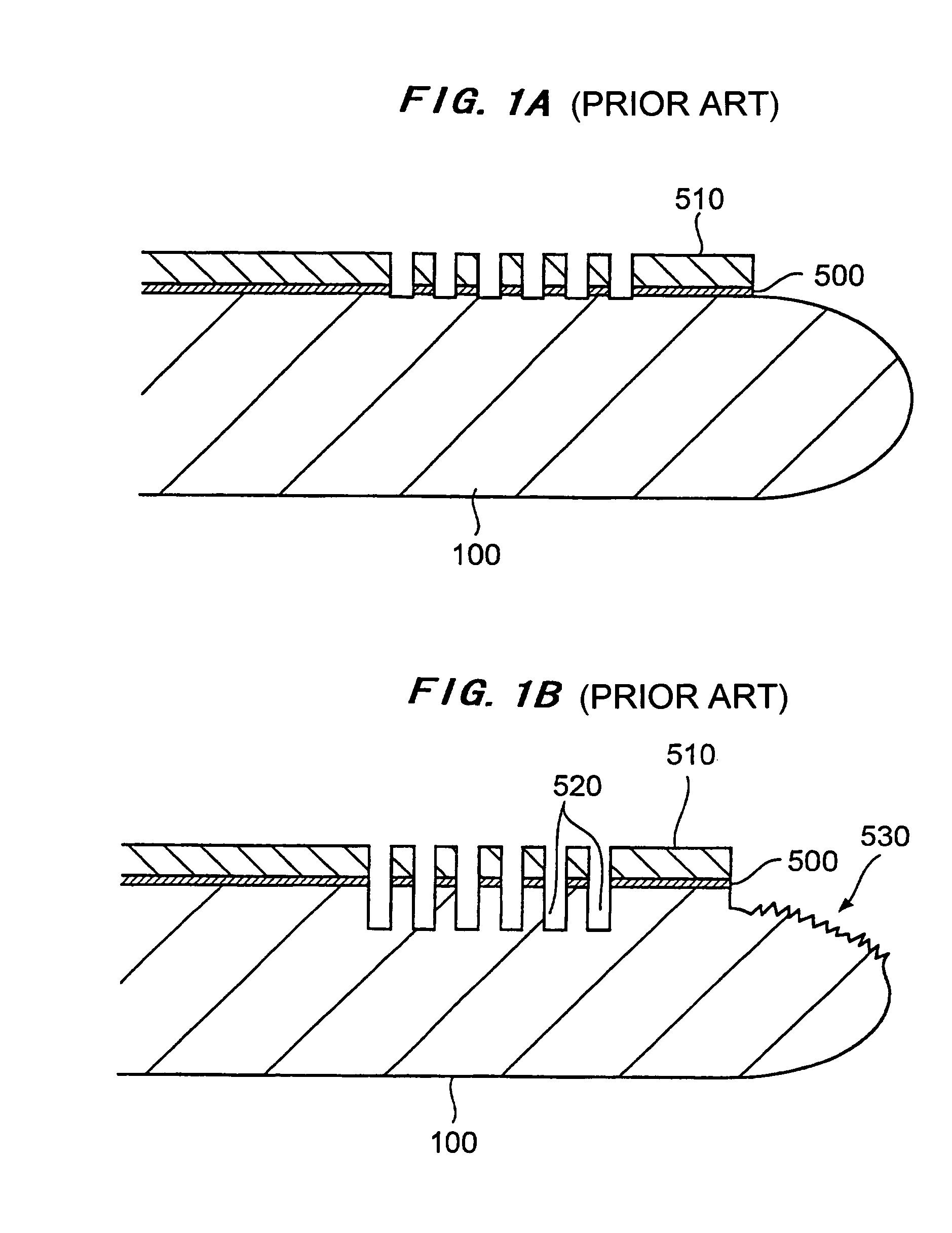
[0088]As shown in FIG. 11, when a Ru film 81 to be used as a lower capacitor electrode is deposited with a thickness of 30 nm on a silicon nitride film 80 deposited on a semiconductor wafer 100 by a batch-type CVD method, the Ru film 81 is deposited not only on a device-formed surface, but also on a bevel portion, an edge portion, and a reverse face with a thickness of about 30 nm. A capacitor using this type of Ru film 81 comprises, for example, a three-dimensional capacitor, and is used for DRAM or FeRAM. As described above, it is necessary to remove the Ru film 81 attached to the bevel portion, the ...

first embodiment

[0089]Therefore, the Ru film attached to the bevel portion, the edge portion, and the reverse face of the semiconductor wafer is removed with use of the substrate processing apparatus of the present embodiment. The substrate processing apparatus in the present embodiment comprises, in addition to a (first) polishing unit described in the first embodiment, a second polishing unit for removing a Ru film 81 attached to a reverse face of a wafer 100. FIG. 12 is a schematic plan view showing the second polishing unit in the present embodiment, and FIG. 13 is a front cross-sectional view of FIG. 12.

[0090]A shown in FIGS. 12 and 13, the second polishing unit comprises a plurality of rollers 11 for rotatably holding a wafer 100, a polishing roll (polishing head) 12 having a polishing film 12b wound on an elastic body 12a, a chemical liquid supply nozzle 13 (not shown in FIG. 13) in the form of a shower nozzle, a support roll 14 made of PVA sponge, and cleaning liquid supply nozzles 15 (not ...

third embodiment

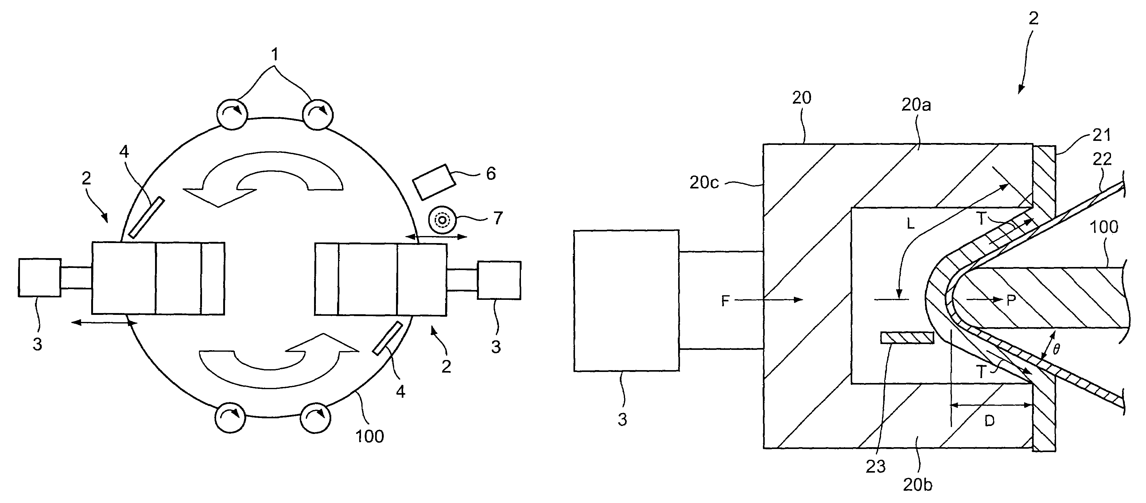
[0106]Next, a substrate processing apparatus according to the present invention will be described below. FIG. 15 is a schematic view showing a polishing head in a substrate processing apparatus according to the present embodiment. As shown in FIG. 15, the polishing head 102 in the present embodiment comprises a support portion 120 having two projecting portions 120a, 120b, and a fluid bag 122 into which a fluid is supplied through a fluid passage 121. The fluid bag 122 is formed of a material having a flexibility, such as thin rubber or soft vinyl, so that it can be deformed in accordance with an internal pressure thereof The fluid passage 121 is connected to a fluid supply source 123, and a fluid such as a gas (air or the like) or a liquid (water or the like) is supplied from the fluid supply source 123 to the fluid bag 122. The fluid supply source 123 can supply a fluid under a desired pressure to the fluid bag 122, and the internal pressure of the fluid bag 122 is adjusted by the...


PUM


Abstract

A substrate processing apparatus has a polishing tape and a polishing head for pressing the polishing tape against a peripheral portion of a semiconductor wafer. The substrate processing apparatus polishes the wafer due to sliding contact of the polishing tape and the wafer. The polishing head has an elastic body for supporting the polishing tape. The substrate processing apparatus has an air cylinder for pressing the polishing head so that the elastic body of the polishing head presses the polishing tape against the predetermined portion of the wafer under a constant force.

Description

BACKGROUND OF THE INVENTION[0001]1. Field of the Invention[0002]The present invention relates to a substrate processing apparatus, and more particularly to a substrate processing apparatus for removing surface roughness produced at a peripheral portion (a bevel portion and an edge portion) or the like of a substrate such as a semiconductor wafer, or for removing a film attached to a peripheral portion or the like of a substrate which would cause contamination.[0003]2. Description of the Related Art[0004]In recent years, according to finer structures of semiconductor elements and higher integration of semiconductor devices, it has become more important to manage particles. One of the major problems in managing particles is dust caused by surface roughness produced at a bevel portion and an edge portion of a semiconductor wafer (substrate) in a manufacturing process of semiconductor devices. In this case, a bevel portion means a portion having a curvature in a cross-section of an edge...

Claims


Application Information

Patent Timeline
Patent Type & Authority Patents(United States)
IPC IPC(8): B24B5/00B24B49/00B24B9/00B24B9/06B24B21/00H01L21/304
CPCB24B9/065B24B21/002
Inventor ISHII, YOUNAKANISHI, MASAYUKINAKAMURA, KENRO
Owner EBARA CORP
Why Eureka
Try Eureka