Method and apparatus for layer by layer deposition of thin films

a thin film and layer deposition technology, applied in chemical vapor deposition coatings, coatings, electric discharge tubes, etc., can solve the problems of difficult implementation in a conventional reactor used for chemical vapor deposition, compromise the wafer throughput, and monolayer of films, so as to increase the wafer throughput for atomic layer processing, increase surface impurities, and increase the effect of alp throughpu

Inactive Publication Date: 2008-07-01
APPLIED MATERIALS INC
View PDF79 Cites 74 Cited by
  • Summary
  • Abstract
  • Description
  • Claims
  • Application Information

AI Technical Summary

Benefits of technology

[0028]A further object of the present invention is to enhance the wafer throughput for atomic layer processing by utilizing a parallel wafer processing module so that the throughput is much higher than single wafer ALP reactors and more competitive with conventional single wafer CVD reactors.
[0029]Yet another object of the present invention is to provide a method for removing impurities from the ALP films without inducing damage or increasing surface impurities by using rapid thermal assisted ALP.
[0030]Briefly, a preferred embodiment of the present invention includes a method of increasing ALP throughput by continuously modulating gas flow in a reactor to achieve layer by layer growth on a wafer. A first reactant is introduced with a percentage of a carrier gas. After a first time interval, the first reactant flow is reduced while the carrier gas flow is increased so as to maintain an approximately constant total gas flow. When the first reactant flow reaches

Problems solved by technology

In this manner, the reaction is usually self-limiting once the surface absorbed reactant is consumed, resulting in a monolayer of the film.
Perfect isolation of the precursors from each other during ALP is not required and in some cases may also be undesirable.
A disadvantage of this method is that it is difficult to implement in a conventional reactor used for chemical vapor deposition, and especially for processes that require high reactant partial pressures over the substrate in order to achieve complete surface saturation.
Cycle times of 10s for conventional ALP also necessitate extremely short pulse and pump—purge times of the order of 2-3 s. As discussed before, cycle times longer than 10 s for single wafer ALP significantly compromise wafer throughput and thus are not production-worthy.
This is achievable for gaseous reactant sources but is more complicated for liquid reactant sources, remote plasma reactant sources, and other sources that respond on the time scales of several seconds.
In addition, reactants diverted into the foreline of the pump are wasted.Repeated rapid cycling of flow components such as flow controllers and valves between the off state and the on state can result in pressure bursts in the chamber and increased particle generation/release in the flow components adversely impacting particle

Method used


Image

  • Method and apparatus for layer by layer deposition of thin films
  • Method and apparatus for layer by layer deposition of thin films
  • Method and apparatus for layer by layer deposition of thin films

Examples


Embodiment Construction

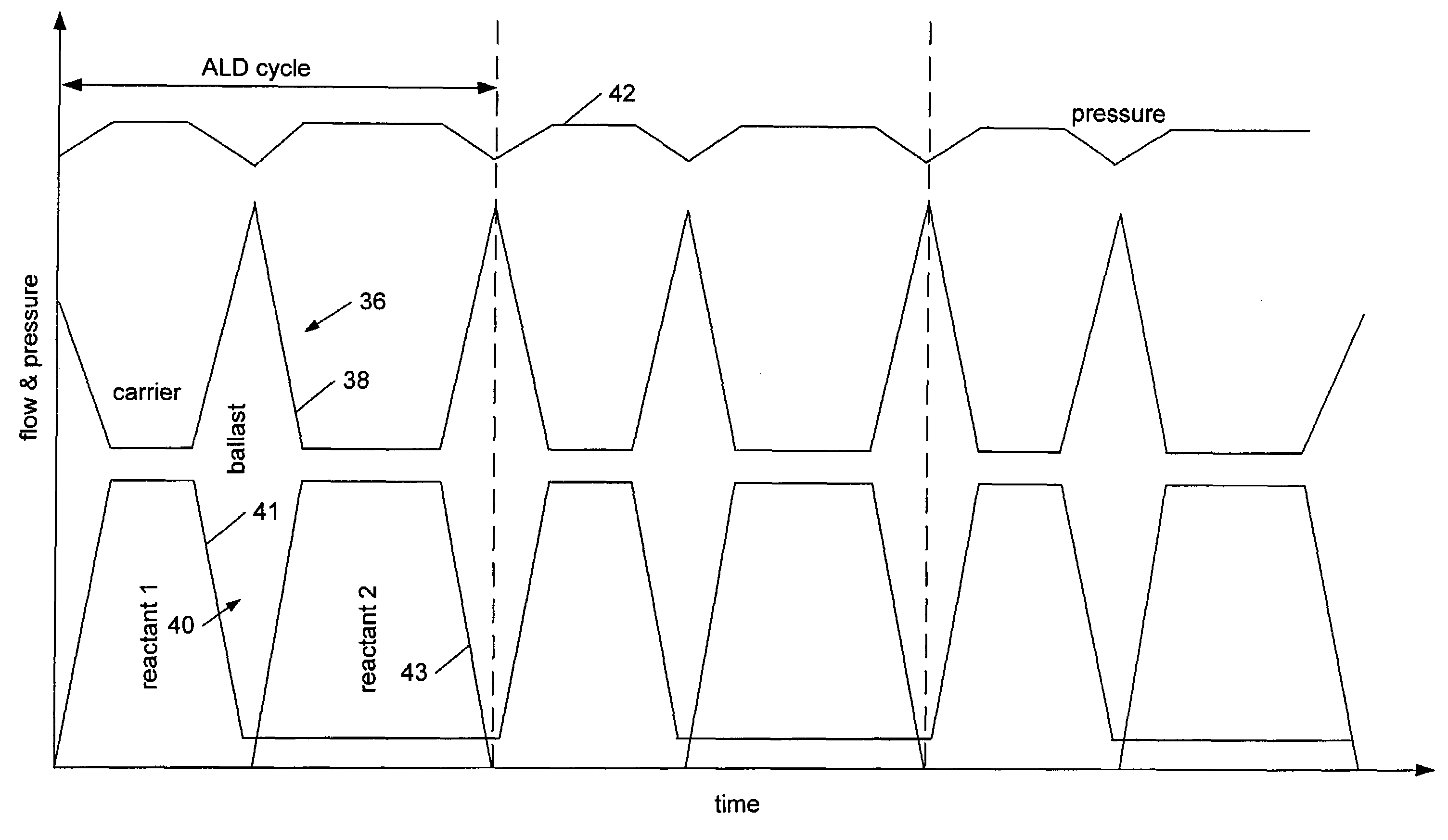
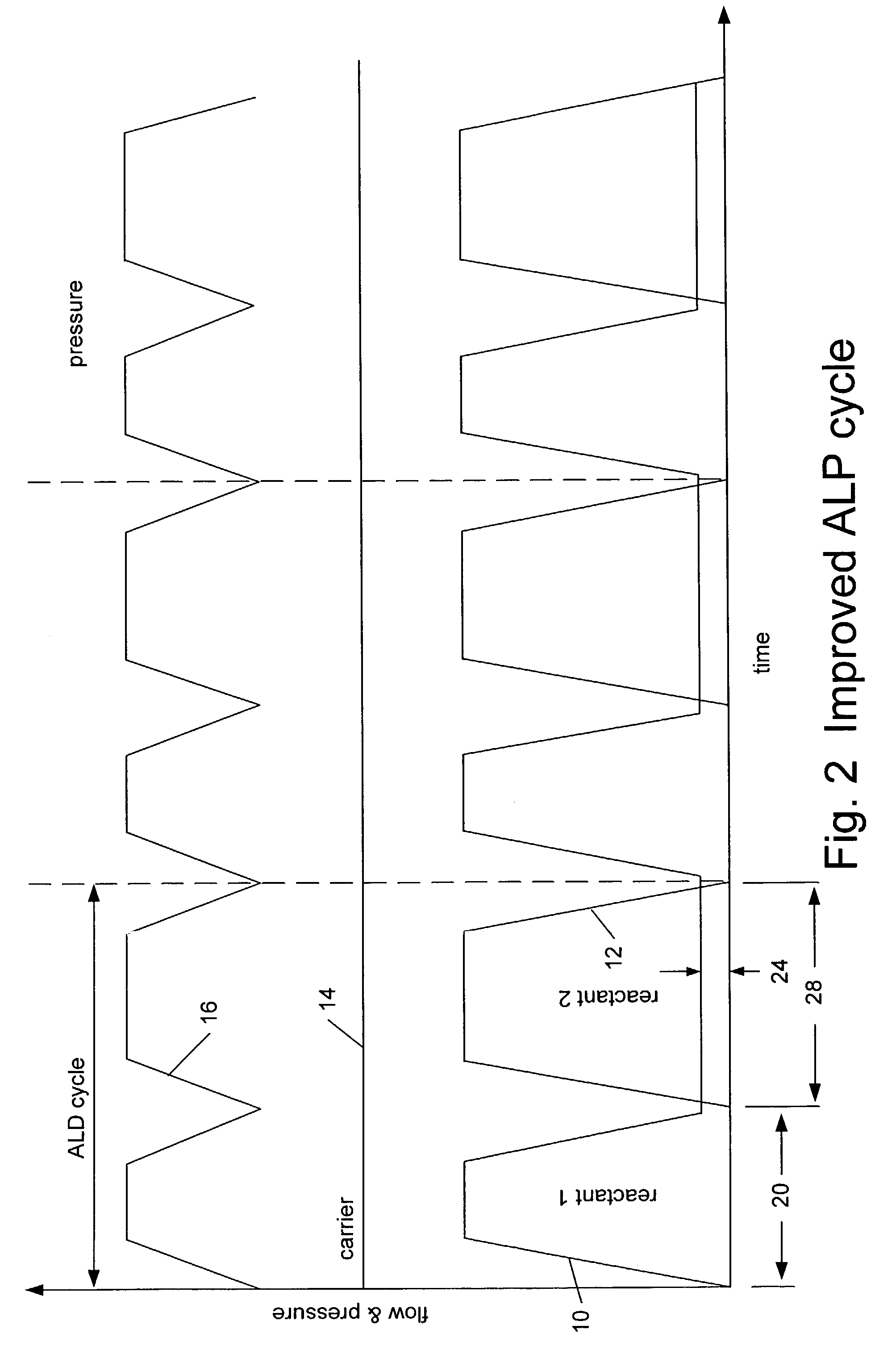
[0054]A preferred embodiment of the method of atomic layer processing of the present invention will now be explained in reference to the graph of FIG. 2 displaying the flow of reactants and a carrier ballast gas as a function of time. Flow of a first reactant gas is illustrated by a curve 10, and a second reactant gas by curve 12. The flow of a ballast / carrier gas is represented by curve 14, and the total gas flow by curve 16. The method of atomic layer processing gas flow is further described in reference to the flow chart of FIG. 3, describing the flow illustrated in FIG. 2. The carrier gas represented by line 14 (FIG. 2) is injected and maintained at a continuous flow rate (block 18). A first reactant gas (line 10, FIG. 2) is then injected according to a predetermined flow modulation contour for a first period of time represented as item 20 in FIG. 2, and as indicated in block 22. The modulation contour shown in FIGS. 2 and 4 is a trapezoidal shape. The present invention also inc...


PUM

PropertyMeasurementUnit
Flow rateaaaaaaaaaa

Abstract

A method of increasing ALP briefly, a preferred embodiment of the present invention includes a method of increasing ALP throughput by continuously modulating gas flow in a reactor to achieve layer by layer growth on a wafer. A first reactant is introduced with a percentage of a carrier gas. After a first time interval, the first reactant flow is reduced while the carrier gas flow is increased so as to maintain an approximately constant total gas flow. When the first reactant flow reaches a minimal, predetermined amount, a second reactant flow is initiated and increased while the carrier gas flow is decreased so as to continue a constant total gas flow. The method alternatively includes introducing a substance that enhances reactant adsorption and chemisorption, either as a first applied gas that reacts with the surface or as an added ligand to the reactant. Still further alternatives include a periodic rapid thermo anneal for improving film properties, parallel wafer processing and a reactant reservoir.

Description

BACKGROUND OF THE INVENTION[0001]1. Field of the Invention[0002]The present invention relates generally to methods and apparatus for deposition of materials on substrates, and more particularly to a method and apparatus for layer by layer deposition of thin films compatible with conventional reactor designs making ALP more amenable to a wider array of reactant sources, ALP reaction chemistries, and reactor geometries without increasing reactor and gas delivery complexity, wherein prior art pump-purge steps are avoided by providing continuously modulated gas flow and pressure, allowing all delivery valves to remain open and diverter lines closed, therefore avoiding rapid cycling of valves between on / off states.[0003]2. Brief Description of the Prior Art[0004]Layer by layer deposition of thin films is becoming increasingly important in semiconductor device fabrication. Layer by layer deposition offers several advantages compared to conventional chemical vapor deposition or chemical va...

Claims


Application Information

Patent Timeline
IPC IPC(8): C23C16/00C23C16/24C23C16/34C23C16/44C23C16/455C23C16/458C23C16/48C23C16/509C23C16/54H01J37/32H01L21/00H01L21/205H01L21/285H01L21/314H01L21/318
CPCC23C16/345H01L21/0262C23C16/45527C23C16/4557H01J37/32082H01J37/32733H01L21/28562H01L21/3141H01L21/3185H01L21/67017H01L21/67069H01L21/67115H01L21/02532C23C16/45525H01J2237/2001H01L21/0228H01L21/0217C23C16/00
Inventor PARANJPE, AJIT P.
Owner APPLIED MATERIALS INC
Why Eureka
Try Eureka