Optical integrated device

a technology of integrated devices and optical components, applied in the field of optical devices, can solve the problems of reducing reducing the performance of the device against the temperature, and inevitably induced reflection of light at the interface, so as to narrow widen the band gap energy of the effect of the effect of widening the effective width of the well layer

Inactive Publication Date: 2008-07-29
SUMITOMO ELECTRIC IND LTD
View PDF12 Cites 6 Cited by
  • Summary
  • Abstract
  • Description
  • Claims
  • Application Information

AI Technical Summary

Benefits of technology

[0014]The first and second active layers may include semiconductor layers composing at least nitrogen (N), or composing at least nitrogen (N), gallium (Ga), and arsenic (As). The first and second active layers may further include at least antimony (Sb) or phosphorous (P). Since semiconductor material composing nitrogen, or at least nitrogen, gallium and arsine may vary the band-gap energy as maintaining a lattice constant thereof matches to that of the GaAs substrate. Therefore, not only a large sized wafer may be applicable to the process but also the band-gap difference between the well and barrier layers may be widened, thereby enhancing the performance of the optical integrated device.
[0016]One preferable structure of the present device includes a ridge in the second cladding layer, and the integrated device may further include a current blocking layer to bury the ridge of the second cladding layer. Even in this structure of the second cladding layer, the first and second active layers may smoothly couple with each other.
[0017]Another preferable structure of the present integrated device provides a mesa including the second cladding layer and the active layer, or additionally including a portion of the first cladding layer. The device may further provide a current blocking layer to bury the mesa. Even in this structure of the second cladding layer, the first and second active layers may smoothly couple with each other. Moreover, since the first and second active layers are limited in a width thereof the mode field diameter of the light in respective active layers becomes substantially identical to each other. Accordingly, the reflection at the interface may be disregarded.
[0020]In the present invention, the diffusing of impurities may be carried out by implanting impurities into the semiconductor layers and by annealing the semiconductor layers. The impurities, which include both extrinsic atoms and vacancies induced by the implantation, may diffuse within the semiconductor layers and reach the active layer to disorder in moderate the quantum well structure, accordingly, to narrow the effective width of the well layers and to widen the band-gap energy thereof.

Problems solved by technology

This means that the band-gap difference between the active layer and layers surrounding the active layer, such as cladding layer and optical confinement layer, is not ensured, thereby reducing the carrier confinement into the active layer and degrading the performance of the device against the temperature.
However, in this butt joint structure, the layer structure in the active device and that in the passive device are occasionally different to each other, at least two structures may not be completely identical in the physical dimensions to each other, so the mode field diameter of the light in the active device and that in the passive device becomes different, accordingly, the reflection of light is inevitably induced at the interface.
However, an extraordinary layer may be formed at the second growth, and this extraordinary layer degrades the interface and the optical coupling thereof which increase the reflection at the interface.
Thus, the butt joint structure lacks the reliability and degrades the performance of the optical integrated device.

Method used


Image

  • Optical integrated device
  • Optical integrated device
  • Optical integrated device

Examples


first embodiment

[0035

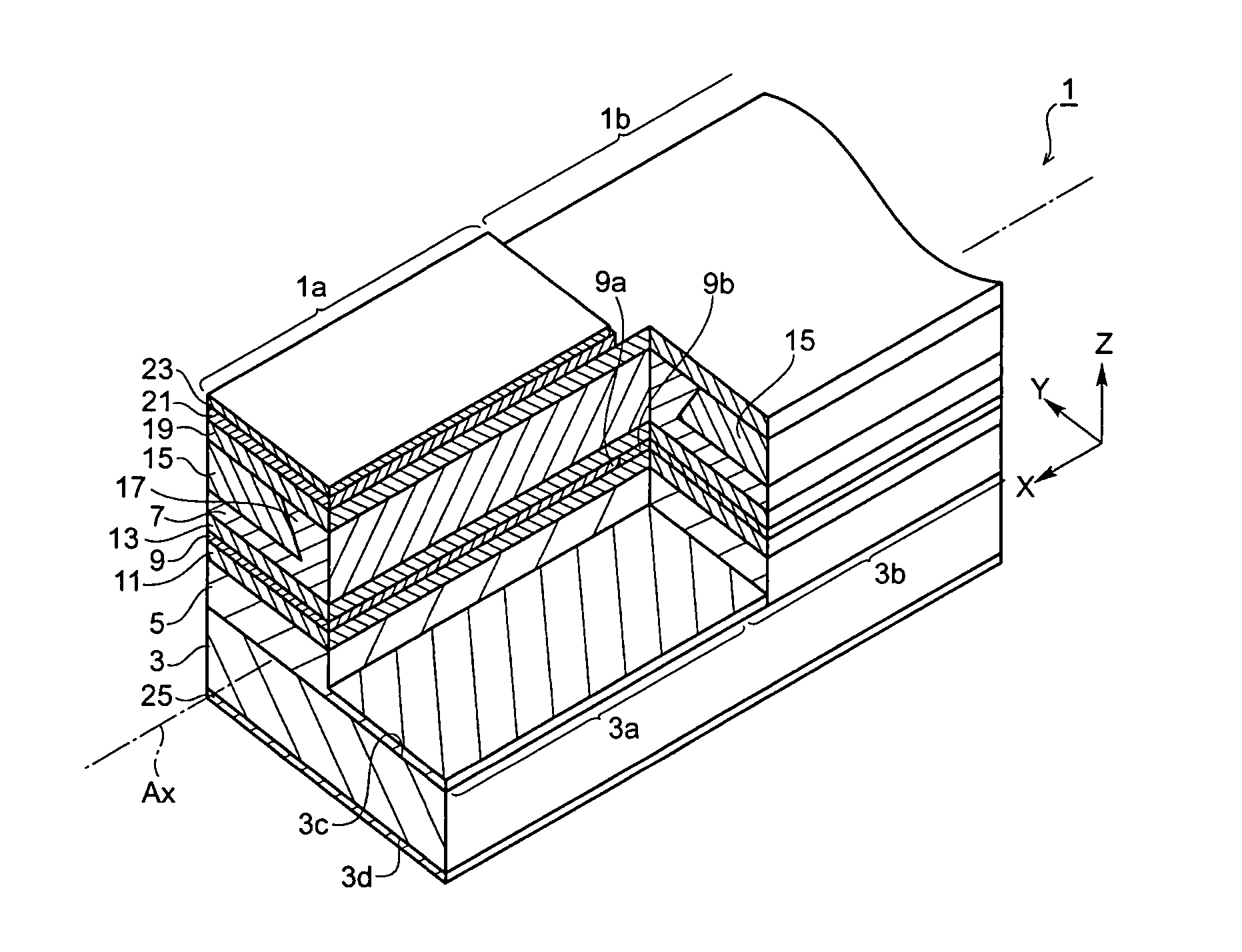
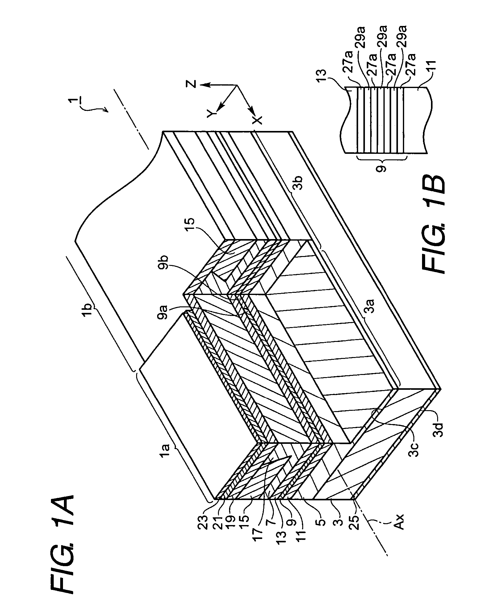
[0036]FIG. 1A is a perspective view showing an optical integrated device 1 according to the present invention, and FIG. 1B is a schematic diagram showing a structure of an active layer of the optical integrated device 1.

[0037]The optical integrated device 1 comprises a GaAs substrate 3, a first cladding layer 5, a second cladding layer 7, and an active layer 9. The GaAs substrate, with a first conduction type and a primary surface 3c of a (100) crystallographic surface, provides a first region 3a where a first device 1a is formed thereon and a second region 3b where a second device 1b is disposed thereon. These first and second regions are arranged along an axis Ax. The first cladding layer 5, showing the first conduction type, is formed in both the first and second regions, 3a and 3b, respectively. The second cladding layer 7, showing a second conduction type, is also formed in the first and second regions, 3a and 3b. The second cladding layer 7, as shown in FIG. 1A, provides ...

second embodiment

[0045

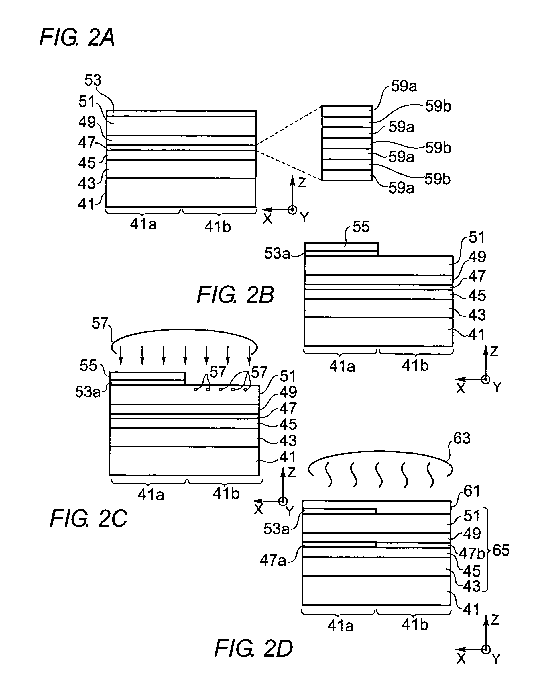
[0046]Next, a process for manufacturing the optical integrated device shown in FIG. 1A will be described as referring to drawings from FIG. 2A to FIG. 2D.

[0047]First, as shown in FIG. 2A, a plurality of semiconductor layers, namely, the first cladding layer 43, the first optical confinement layer 45, the active layer 47, the second optical confinement layer 49, the second cladding layer 51, and the cap layer 53 are grown on a GaAs wafer 41 by the Organo-Metallic Vapor Phase Epitaxy (OMVPE) technique. The first cladding layer 43 has the first conduction type, while the second cladding layer 51 has the second conduction type. The active layer 47, as described previously, has the multi-quantum well structure with a plurality of well layers and barrier layers alternately stacked to each other. The cap layer 53, which covers semiconductor layers formed thereunder, is GaAs. The semiconductor layers for the first device la is provided on the first region 41a, while the layers for the ...

third embodiment

[0074

[0075]FIG. 8A is a perspective view showing another optical integrated device 101 according to the third embodiment of the invention, and FIG. 8B is a schematic diagram showing a layer structure of an active layer of the device shown in FIG. 8A .

[0076]The optical integrated device 101 provides a similar structure to those shown in the previously explained device 1 except that the active layer 109, the first and second cladding layers, 105 and 107, and the upper and lower optical confinement layers, 111 and 113, form a mesa 117, while only the upper cladding layer makes the ridge in the first embodiment.

[0077]Similar to the previous embodiment, the mesa 117 extends from the first region 3a to the second region 3b. The active layer 109a in the first device 101a also smoothly continues to the second active layer 109b. Both the first and second active layers, 109a and 109b, are sandwiched by the first and second optical confinement layers, 111 and 113, in respective regions, 101a a...


PUM


Abstract

The present invention provides an optical device integrating an active device with a passive device without any butt joint structure between two devices. The optical integrated device of the invention includes a GaAs substrate, first and second cladding layers, and an active layer sandwiched by the first and second cladding layers. These layers are disposed on the GaAs substrate. The GaAs substrate provides a first region and a second region. The active layer comprises of the first active layer disposed on the first region and the second active layer disposed on the second region of the GaAs substrate. The first active layer has a quantum well structure whose band-gap energy smaller than 1.3 eV, while the second active layer has a quantum well structure whose band-gap energy is greater than that of the first active layer.

Description

BACKGROUND OF THE INVENTION[0001]1. Field of the Invention[0002]The present invention relates to an optical device that monolithically integrates an optically active device and an optically passive device.[0003]2. Related Prior Art[0004]Japanese patent published as S63-196088 has disclosed a semiconductor laser diode, an edge portion of which is widened in the band-gap energy by the diffusion of zinc (Zn) atoms. This edge portion functions as a window region for the coherent light. This window region with widened band-gap energy may prevent the laser from the COD (Catastrophic Optical Damage) and the degradation thereby.[0005]Japanese patent published as 2001-148531 has disclosed an optically integrated device that includes an optical waveguide and an optical amplifier both provided on single GaAs substrate. The optical amplifier, optically coupled with the optical waveguide, comprises of an active layer made of GaxIn1-xNyAs1-y, first and second cladding layers sandwiching the activ...

Claims


Application Information

Patent Timeline
Patent Type & Authority Patents(United States)
IPC IPC(8): H01L29/06H01S5/026G02B6/12G02B6/122G02B6/13H01S5/16H01S5/22H01S5/223H01S5/227H01S5/32H01S5/343
CPCB82Y20/00G02B6/122G02B6/131H01S5/026H01S5/162H01S5/2231H01S5/227G02B2006/121H01S5/3434H01S5/2223H01S5/2224H01S5/3211H01S5/34306H01S5/222
Inventor HASHIMOTO, JUN-ICHIKATSUYAMA, TSUKURUKOYAMA, KENJI
Owner SUMITOMO ELECTRIC IND LTD
Why Eureka
Try Eureka