Modulated temperature method of atomic layer deposition (ALD) of high dielectric constant films

a technology of atomic layer deposition and dielectric constant, which is applied in the direction of chemical vapor deposition coating, coating, coating process, etc., can solve the problems of high leakage of silicon dioxide films less than 1.5 nm, inability to use gate dielectrics in fet devices, and high power consumption, so as to achieve the effect of efficiently removing excess ligands and so great ligand buildup

Active Publication Date: 2008-10-28
SHARP KK
View PDF10 Cites 30 Cited by
  • Summary
  • Abstract
  • Description
  • Claims
  • Application Information

AI Technical Summary

Benefits of technology

[0021]It is an object of the invention to provide a very uniform deposition of dense metal oxide films at low temperatures.
[0022]Another object of the invention is to provide a method of efficiently removing excess ligands before the ligand buildup is so great that the ligands cannot all be removed by a post deposition anneal.
[0023]Another object of the invention to provide a very uniform deposition of dense metal oxide films without use of an oxidizing species, such as oxygen or water.
[0024]It is a further object of the invention to provide a very uniform deposition of dense hafnia films at low temperature without use of an oxidizing species such as oxygen or water.

Problems solved by technology

Silicon dioxide films of less than 1.5 nm have a high leakage from direct tunneling currents and generally cannot be used as a gate dielectric in FET devices because of excessive power consumption.
Other fabrication and reliability concerns of very thin silicon dioxide films include boron penetration and charge injection damage.
As the gate oxide thickness is scaled below 1.5 nm, problems arise, such as excessive power consumption due to current leakage from direct tunneling, boron dopant penetration, reliability concerns, etc.
So far, a suitable replacement for SiO2 has not been found.
Thus many useful CVD precursors are not viable as ALD precursors and vice versa.
Metal organics have the potential to introduce organic contamination into the IC structure during the fabrication process, leading to degraded IC performance.
HfO2 and ZrO2 films deposited using a metal halide precursor, such as [M+]Cl4, demonstrate good insulating properties, including high dielectric constant and low leakage, however, they do not provide smooth deposition directly on H-terminated silicon and require several “incubation” cycles, which may result in roughening.
Because even a very thin low-k layer can negate most of the benefits of an overlying high-k layer, the presence of several monolayers of SiO2 makes it difficult to achieve EOT<1.0 nm using this type of precursor.
In addition, films produced by all of the above-described methods suffer from poor channel mobility when integrated into an MOS device structure.
Yet another problem with traditional method of ALD is the presence of silicon oxide at the wafer interface.
The use of water vapor introduces a number of problems: The introduction of the necessary quantity of water vapor is difficult to control, and typically, an abundance of water vapor is introduced into the chamber.
Desorption of water vapor, e.g., via vacuum pumping, adds considerable time to the overall process time, reducing the throughput.

Method used


Image

  • Modulated temperature method of atomic layer deposition (ALD) of high dielectric constant films
  • Modulated temperature method of atomic layer deposition (ALD) of high dielectric constant films
  • Modulated temperature method of atomic layer deposition (ALD) of high dielectric constant films

Examples


example

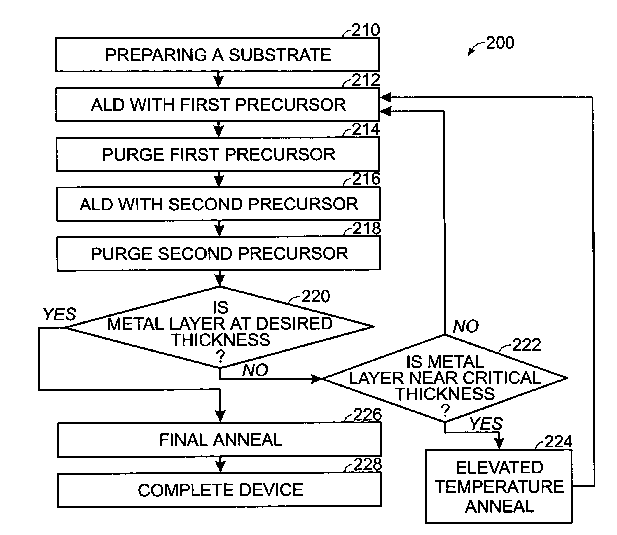
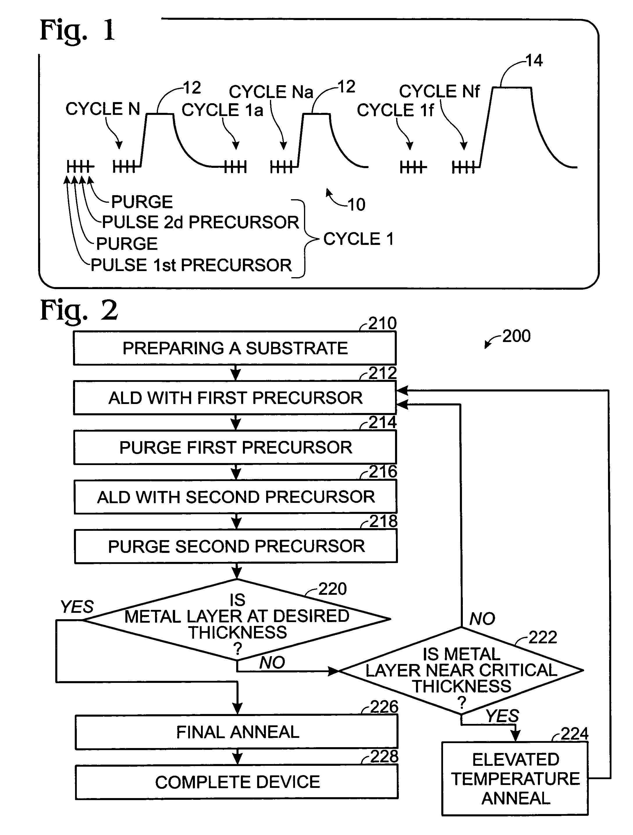
[0060]An example of demonstrated utility of the method of the invention follows: HfO2 films were deposited on H-terminated silicon using 10, 15, and 45 cycles of Hf(NO3)4 / HfCl4 / and periodic elevated temperature anneal, as described above. The resulting films were visually uniform. In this example, the films were annealed after every ALD cycle, e.g., N=1. Control films were also deposited in which the films were annealed only after the deposition was complete.

High Deposition Rate, Directly on H-terminated Silicon

[0061]Thickness was measured via spectroscopic ellipsometry. A plot of optical thickness at the center of the wafer vs. the number of deposition cycles is depicted in FIG. 8, and demonstrates that thickness is linearly dependent on the number of deposition cycles. Thickness variation was less than + / −5% over a 6″ wafer. The fact that the linear fit in the plot below does not intersect the x-axis confirms ease of deposition on H-terminated silicon. From the slope of the curve...


PUM

PropertyMeasurementUnit
thicknessaaaaaaaaaa
temperatureaaaaaaaaaa

Abstract

A method of forming a layer of high-k dielectric material in an integrated circuit includes preparing a silicon substrate; forming a high-k dielectric layer by a sequence of ALD cycles including: depositing a first layer of metal ligand using ALD with an oxygen-containing first precursor; and depositing a second layer of metal ligand using ALD with a second precursor; repeating the sequence of ALD cycles N times until a near-critical thickness of metal oxide is formed; annealing the substrate and metal oxide layers every N ALD cycles in an elevated temperature anneal; repeating the sequence of ALD cycles and elevated temperature anneals until a high-k dielectric layer of desired thickness is formed; annealing the substrate and the metal oxide layers in a final annealing step; and completing the integrated circuit.

Description

RELATED APPLICATIONS[0001]This application is related to application Ser. No. 09 / 894,941, filed Jun. 28, 2001, for Methods of using atomic layer deposition to deposit a high dielectric constant material on a substrate, now U.S. Pat. No. 6,420,279 B1, granted Jul. 16, 2002; application Ser. No. 10 / 286,100, filed Oct. 31, 2002, for Method to deposit a stacked high k gate dielectric for CMOS applications now U.S. Pat. No. 6,686,212 B1, granted Feb. 3, 2004, application Ser. No. 10 / 376,774, filed Feb. 27, 2003, for Two precursor method to perform atomic layer deposition (ALD) of a stacked high-k gate dielectric for CMOS applications now abandoned, and application Ser. No. 10 / 376,794, filed Feb. 27, 2003, for Method for depositing a nanolaminate film by atomic layer deposition, now U.S. Pat. No. 6,930,059 B1, granted Aug. 16, 2005.FIELD OF THE INVENTION[0002]This invention relates to a method for deposition of uniform ceramic films for a wide range of applications, such as optical coatin...

Claims


Application Information

Patent Timeline
Patent Type & Authority Patents(United States)
IPC IPC(8): C23C16/00C23C16/44C23C16/455C23C16/56H01L21/314H01L21/316
CPCC23C16/45527C23C16/56H01L21/3141H01L21/31641H01L21/31645H01L21/31604H01L21/31616H01L21/31637H01L21/02205H01L21/0228H01L21/02181H01L21/02318
Inventor CONLEY, JR., JOHN F.ONO, YOSHISTECKER, GREGORY M.
Owner SHARP KK
Why Eureka
Try Eureka