Beam irradiation apparatus, beam irradiation method, and method for manufacturing thin film transistor

a technology of beam irradiation and beam irradiation, which is applied in the direction of transistors, manufacturing tools, solid-state devices, etc., can solve the problems of long irradiation time, difficult laser processing uniformity, and inability to accurately detect the speed of laser light scanned with scanning means such as galvanometer mirrors or polygon mirrors

Inactive Publication Date: 2009-01-13
SEMICON ENERGY LAB CO LTD
View PDF66 Cites 6 Cited by
  • Summary
  • Abstract
  • Description
  • Claims
  • Application Information

AI Technical Summary

Problems solved by technology

Such a region makes it difficult to perform the laser processing uniformly.
Moreover, the speed of the laser light scanned with the scanning means such as the galvanometer mirror or the polygon mirror is not constant in the center portion and in the end portion of the scanning width.
In such a region where the scanning speed decelerates, accelerates, and becomes zero, the irradiation time becomes longer so that the object to be irradiated is irradiated with excessive en...

Method used


Image

  • Beam irradiation apparatus, beam irradiation method, and method for manufacturing thin film transistor
  • Beam irradiation apparatus, beam irradiation method, and method for manufacturing thin film transistor
  • Beam irradiation apparatus, beam irradiation method, and method for manufacturing thin film transistor

Examples


embodiment mode 1

[0036]This embodiment mode explains a beam irradiation method and an apparatus for irradiating the beam (a beam irradiation apparatus) specifically with reference to FIGS. 3A and 3B.

[0037]First, as shown in FIG. 3A, a beam spot 31 is scanned on an object to be irradiated 32 by the scanning means. Initially, the beam spot 31 is scanned to a first direction of the minor axis (A1) and then the beam spot 31 is scanned to a direction of the major axis (B1). After that, the beam spot 31 is scanned to a second direction of the minor axis (A2) and then the beam spot 31 is scanned to the direction of the major axis (B1) again. When such an operation is repeated, a wide range of the object to be irradiated can be scanned with the beam spot 31. On this occasion, for example, the first scanning means scan in the direction of the minor axis and the second scanning means scan in the direction of the major axis. The second scanning means correspond to a moving of the object to be irradiated by a s...

embodiment mode 2

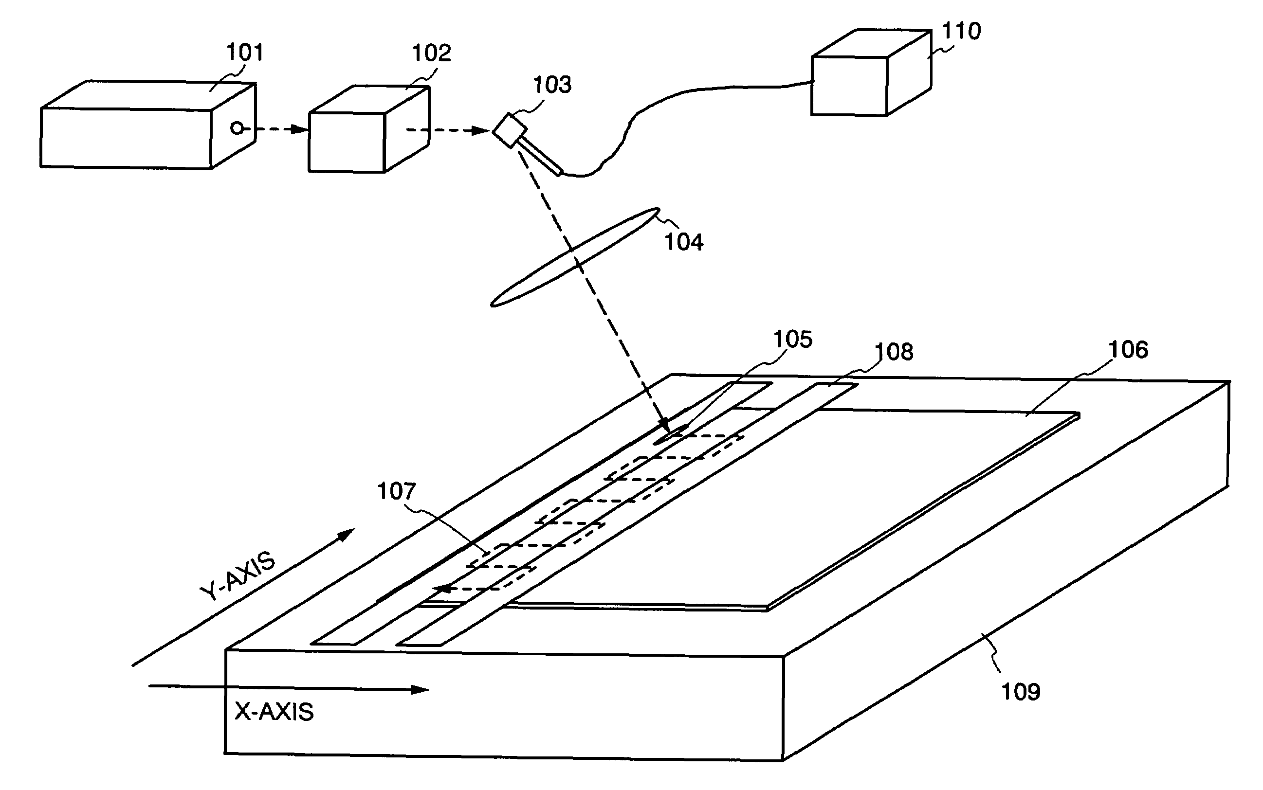
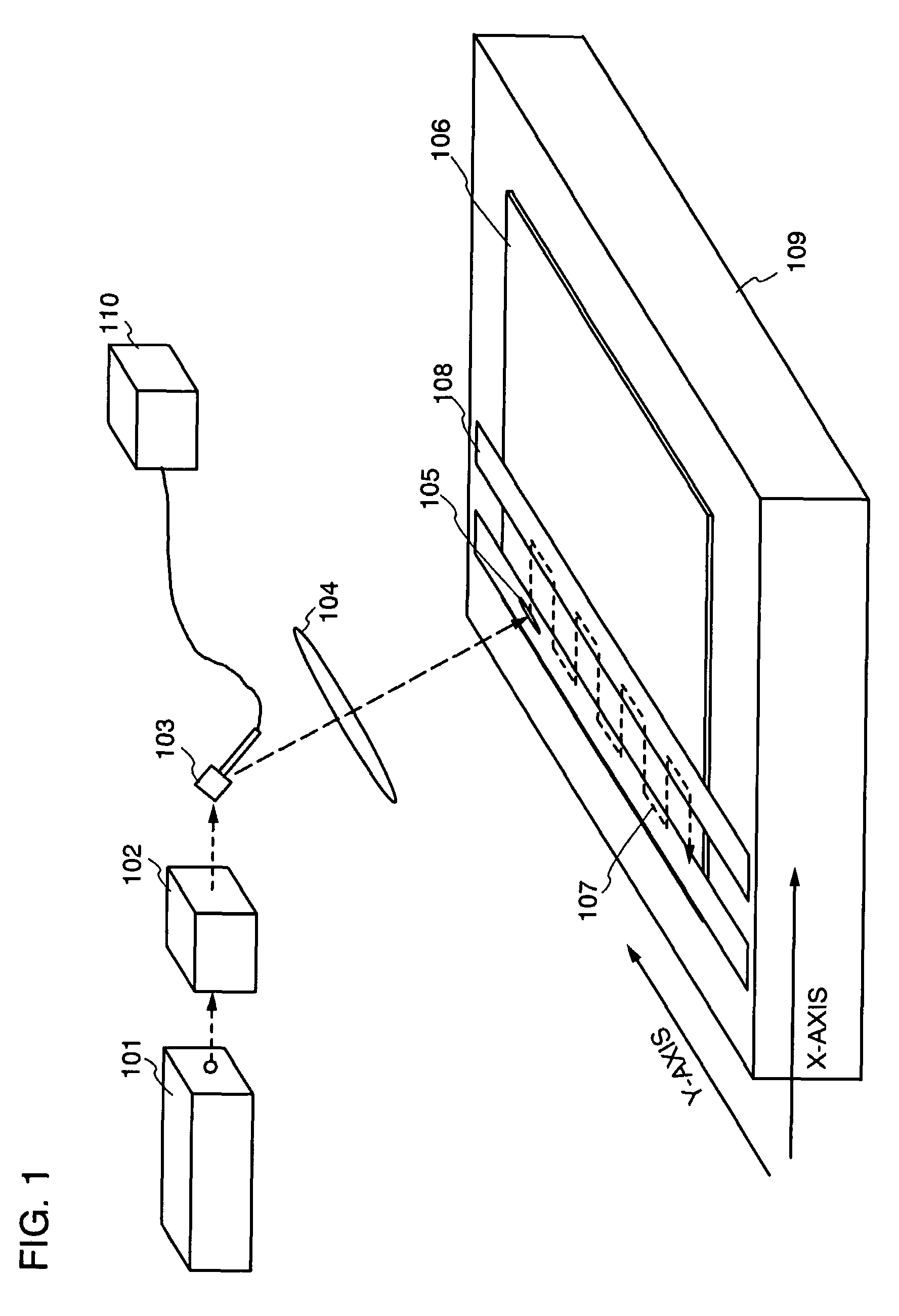
[0049]This embodiment mode explains a laser irradiation apparatus and a laser irradiation method using a CW laser as one mode of the beam with reference to FIG. 1. In addition, this embodiment mode explains the case where the semiconductor film is used as the object to be irradiated and the galvanometer mirror is used as the first scanning means.

[0050]First, a CW laser emitted from a laser oscillator 101 is extended long through an optical system 102 and is shaped into linear. Specifically, the laser can be shaped into linear after transmitting through a cylindrical lens and a convex lens included in the optical system 102.

[0051]After that, the laser shaped into linear (hereinafter referred to as a linear laser) is incident into the semiconductor film 106 through a galvanometer mirror 103 and an fθ lens 104. The linear laser here is adjusted so that a laser beam spot 105 having the predetermined size is formed on the semiconductor film. In addition, the fθ lens 104 can make the lase...

embodiment mode 3

[0066]This embodiment mode explains the case to enhance productivity of the thin film transistor by performing the laser annealing, that is, the laser processing with a plurality of laser oscillators to the semiconductor film formed over the substrate.

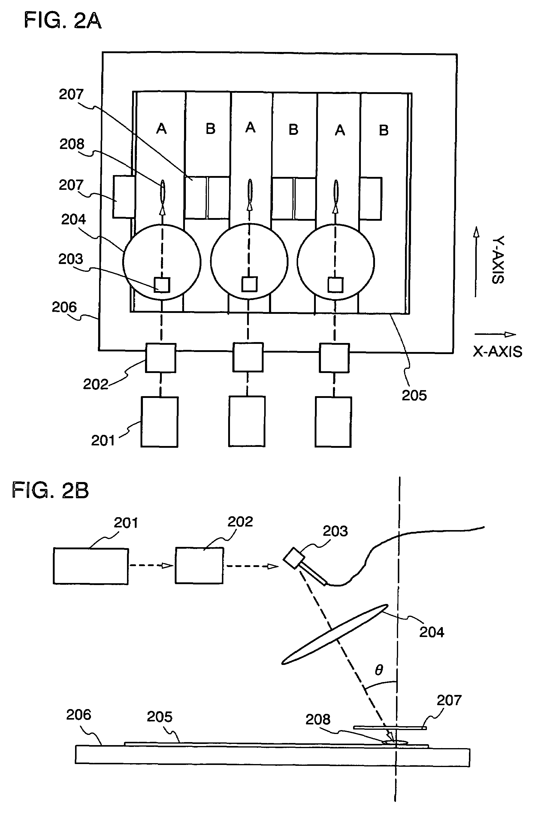
[0067]FIGS. 2A and 2B show an example to employ three laser oscillators 201, three telecentric fθ lenses 204, three galvanometer mirrors 203, and three pairs of slits 207 are employed to perform the laser annealing to the semiconductor film 205 formed over a large-sized substrate having a size of 1500 mm×1800 mm. It is noted that FIG. 2A is a top view and FIG. 2B is a side view.

[0068]An oxide film (a silicon oxide film such as SiON or SiO2) is formed over a substrate as a base film and then a semiconductor film is formed thereon sequentially. The semiconductor film may be formed of the material mainly consisting of silicon with CVD, sputtering, or the like. In this embodiment mode, an amorphous silicon film is formed with the CVD using...


PUM

PropertyMeasurementUnit
Lengthaaaaaaaaaa
Distanceaaaaaaaaaa
Speedaaaaaaaaaa

Abstract

The speed of the laser scanned with the scanning means such as a galvanometer mirror or the polygon mirror is not constant in the center portion and in the end portion of the scanning width. As a result, the object to be irradiated is irradiated with the excessive energy and thereby there is a risk that the amorphous semiconductor film may be peeled.
In the case of scanning the spot of the energy beam output continuously with the scanning means, the present invention is to block the CW beam irradiated to the regions in the object to be irradiated where the scanning speed of the spot accelerates, decelerates, and it becomes zero, that is to say, when the spot is in the position where the scanning starts and in the position where the scanning ends.

Description

BACKGROUND OF THE INVENTION[0001]1. Field of the Invention[0002]The present invention relates to a beam irradiation apparatus and a beam irradiation method. Moreover, the present invention relates to a method for manufacturing a thin film transistor using the beam irradiation apparatus and the beam irradiation method.[0003]2. Related Art[0004]The research has been conducted on a thin film transistor having a poly-crystalline semiconductor film in its channel-forming region (hereinafter referred to as a poly-crystalline TFT) as a semiconductor element included in a display device, an integrated circuit, or the like. With the development of the display device and the integrated circuit, further enhancement of the characteristic of the poly-crystalline TFT is expected.[0005]Consequently, in order to enhance the characteristic of the poly-crystalline TFT, crystallization of the semiconductor film by continuous wave (CW) laser light is examined. For example, there is a method for crystal...

Claims


Application Information

Patent Timeline
IPC IPC(8): H01L21/00B23K26/06B23K26/08H01L21/20H01L21/336H01L21/77H01L21/84H01L27/12H01L29/786
CPCB23K26/0656B23K26/08B23K26/0807B23K26/0815H01L21/2026H01L27/12H01L29/66757H01L29/78675H01L27/1285B23K26/0821B23K26/082B23K26/066H01L21/02592H01L21/02683H01L21/02422H01L21/02488H01L21/0242H01L21/02425H01L21/02686H01L21/02678H01L21/02532H01L21/02595H01L21/02381H01L21/02691
Inventor TANAKA, KOICHIRO
Owner SEMICON ENERGY LAB CO LTD
Why Eureka
Try Eureka