Method for controlling the structure and surface qualities of a thin film and product produced thereby

a technology of structure and surface quality, applied in the direction of lasers, semiconductor lasers, semiconductor devices, etc., to achieve the effects of improving device performance and longevity, improving surface quality, and improving structural quality

Inactive Publication Date: 2009-03-10
PALO ALTO RES CENT INC
View PDF19 Cites 35 Cited by
  • Summary
  • Abstract
  • Description
  • Claims
  • Application Information

AI Technical Summary

Benefits of technology

[0015]Optical devices produced by the method of the present invention exhibit efficient UV light extraction through a lowermost structural layer, such as a UV-transparent AlGaN current spreading layer. Lower operating voltages are also provided due to the lack of high series resistance layers and the vertical orientation of the device. Non-optical devices produced by the method of the present invention exhibit layers (e.g., active layers) having improved structural quality, and hence device performance and longevity.

Problems solved by technology

Lower operating voltages are also provided due to the lack of high series resistance layers and the vertical orientation of the device.

Method used


Image

  • Method for controlling the structure and surface qualities of a thin film and product produced thereby
  • Method for controlling the structure and surface qualities of a thin film and product produced thereby
  • Method for controlling the structure and surface qualities of a thin film and product produced thereby

Examples


Embodiment Construction

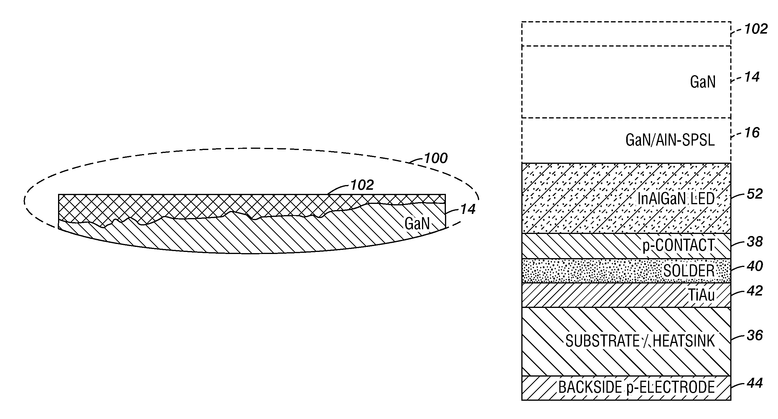
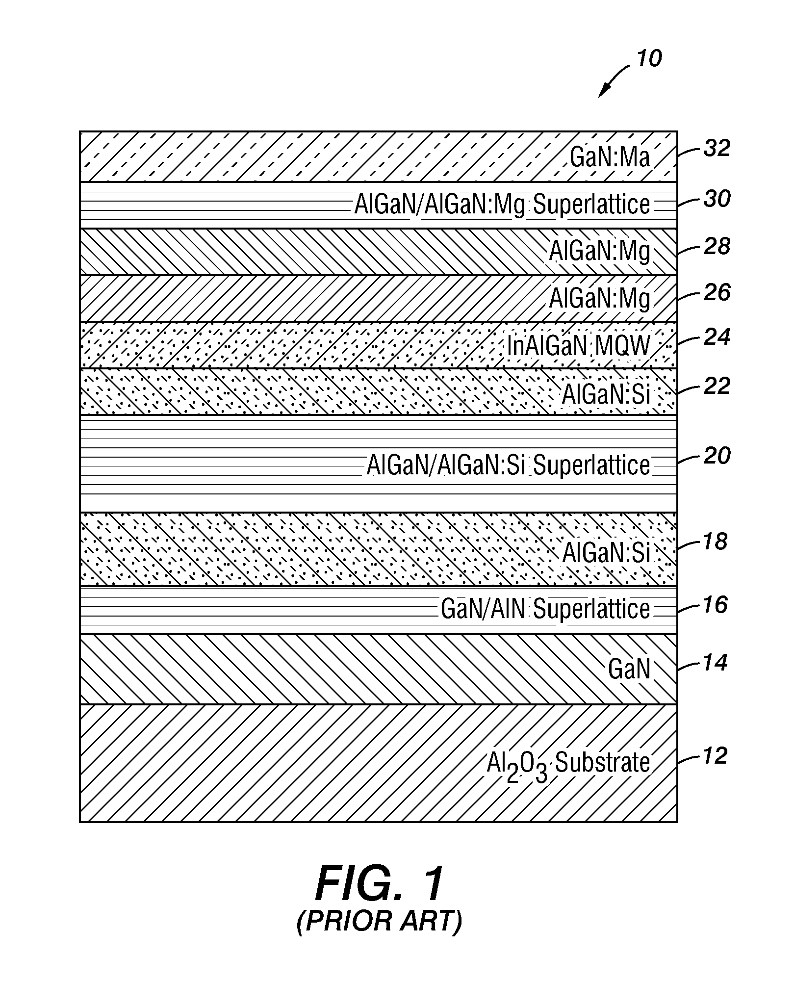
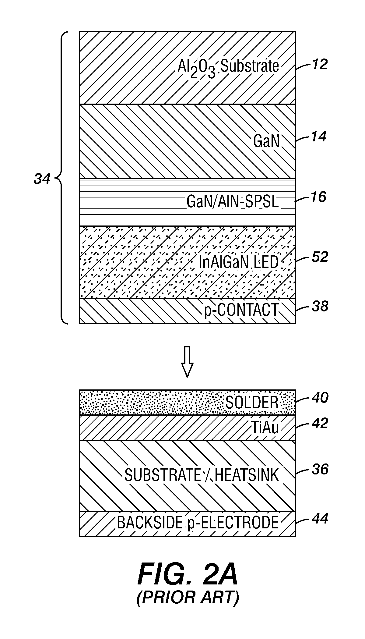
[0026]For the purposes of explanation, the present invention will be described and illustrated staring with a foundation of a known device such as an InAlGan multiple quantum well heterostructure light emitting diode of the type illustrated in FIG. 1. It will be appreciated that the present invention finds applicability, however, with regard to many other structures such as semiconductor lasers, and many other systems such as those employing InGaN or other materials as intermediate, active (non-optical) or light emitting layers. With regard then to FIG. 1, and the exemplary LED illustrated therein, index guided, buried heterostructure AlGalnN light emitting diode structure 10 comprises an Al2O3 (sapphire) substrate 12 on which is formed a 2-10 micron thick epitaxial GaN template layer 14. GaN template layer 14 can be Si-doped or undoped and is typically grown at approximately 1100 degree C. and a reactor pressure of approximately 200 Torr. Formed thereon is a GaN / AlN short period su...


PUM

PropertyMeasurementUnit
wavelengthsaaaaaaaaaa
external quantum efficienciesaaaaaaaaaa

Abstract

A system and method for providing improved surface quality following removal of a substrate and template layers from a semiconductor structure provides an improved surface quality for a layer (such as a quantum well heterostructure active region) prior to bonding a heat sink / conductive substrate to the structure. Following the physical removal of a sapphire substrate, a sacrificial coating such as a spin-coat polymer photoresist is applied to an exposed GaN surface. This sacrificial coating provides a planar surface, generally parallel to the planes of the interfaces of the underlying layers. The sacrificial coating and etching conditions are selected such that the etch rate of the sacrificial coating approximately matches the etch rate of GaN and the underlying layers, so that the physical surface profile during etching approximates the physical surface profile of the sacrificial coating prior to etching. Following etching, a substrate is bonded to the exposed surface which acts as a heat sink and may be conductive providing for backside electrical contact to the active region.

Description

CROSS-REFERENCE TO RELATED APPLICATIONS[0001]The present invention is related to provisional U.S. Applications for Letters Patent titled “Superlattice Strain Relief Layer For Semiconductor Devices”, Ser. No. U.S. 60 / 736,362, and “Method For Controlling The Structure And Surface Qualities Of A Thin Film And Product Produced Thereby”, Ser. No. U.S. 60 / 736,531, each filed on Nov. 14, 2005, each assigned to the same assignee as the present application, and each being incorporated by reference herein.BACKGROUND OF THE INVENTION[0002]1. Field of the Invention[0003]The present invention is related generally to the field of solid state light emitting diode and laser fabrication, and more particularly to techniques for controlling the structure and surface qualities of layers of such structures for improved device performance, reliability, and lifespan.[0004]2. Description of the Prior Art[0005]In the III-V compound semiconductor family, the nitrides have been used to fabricate visible wavel...

Claims


Application Information

Patent Timeline
Patent Type & Authority Patents(United States)
IPC IPC(8): H01L21/00
CPCB82Y20/00H01L33/0079H01S5/0213H01S5/0216H01S5/0217H01S5/32341H01S5/34333H01L33/0093
Inventor WONG, WILLIAM S.KNEISSL, MICHAEL A.TEEPE, MARK
Owner PALO ALTO RES CENT INC
Why Eureka
Try Eureka