Molecular beam epitaxy growth of ternary and quaternary metal chalcogenide films

a technology of ternary and quaternary metals and chalcogenide, which is applied in the field of epitaxy growth of cdsexte1x and cdsexte1x on silicon, can solve the problems of low defect level, difficult growth of suitable crystal quality cdznte layers, and failure to disclose the mbe growth of high quality cdsete and cdznsete films on silicon based substrates, etc., and achieve excellen

Inactive Publication Date: 2009-04-14
UNITED STATES OF AMERICA THE AS REPRESENTED BY THE SEC OF THE ARMY
View PDF7 Cites 17 Cited by
  • Summary
  • Abstract
  • Description
  • Claims
  • Application Information

AI Technical Summary

Benefits of technology

[0010]CdSeTe is grown on Si at different growth temperatures. The rate of Se incorporation tends to be higher than the rate of Te incorporation, particularly sa the growth temperature is increased. As-grown CdSeTe with a 4% Se content (CdSe0.04Te0.96) exhibited excellent surface morphology, low surface defect density (less than 500 cm−2) and a low X-ray double crystal rocking curve (DCRC) full-width at half maximum (FWHM) of 103 arcsec or better. As-grown CdZnSeTe layer with 4% of Zn+Se contents exhibited excellent surface morphology, low surface defect density (less than 500 cm−2) and low X-ray DCRC FWHM of 101 arcsec. These compositions are lattice matched to long-wavelength infrared (LWIR) HgCdTe material, allowing fabrication of improved IR detectors and other devices.

Problems solved by technology

However, it is difficult to growth CdZnTe layers of suitable crystal quality and low defect levels on Si.
Furthermore, the crystalline structure of Cd1-zZnzTe degrades for increasing values of z, perhaps due to a miscibility gap.
However, the prior art fails to disclose the MBE growth of high quality CdSeTe and CdZnSeTe films on a silicon based substrate, having low surface defect density and potential lattice matching to HgCdTe.

Method used


Image

  • Molecular beam epitaxy growth of ternary and quaternary metal chalcogenide films
  • Molecular beam epitaxy growth of ternary and quaternary metal chalcogenide films
  • Molecular beam epitaxy growth of ternary and quaternary metal chalcogenide films

Examples


Embodiment Construction

[0026]The present invention has utility in infrared communication, infrared sensor and infrared imaging device construction. While the present invention is detailed herein with respect to CdSexTe1-x, and Cd1-zZnzSexTe1-x, it is appreciated that the exemplary teachings for these specific ternary and quaternary cadmium chalcogenides are readily extended to CdSxTe1-x, Cd1-zZnzSxSe1-x and Cd1-zZnzSxTe1-x.

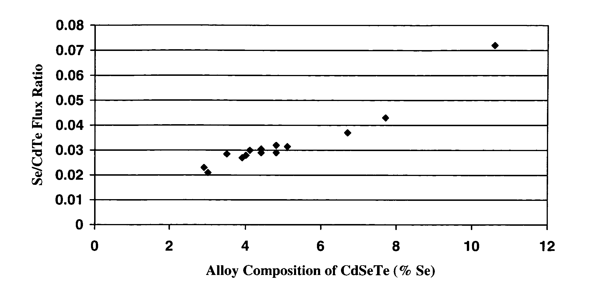
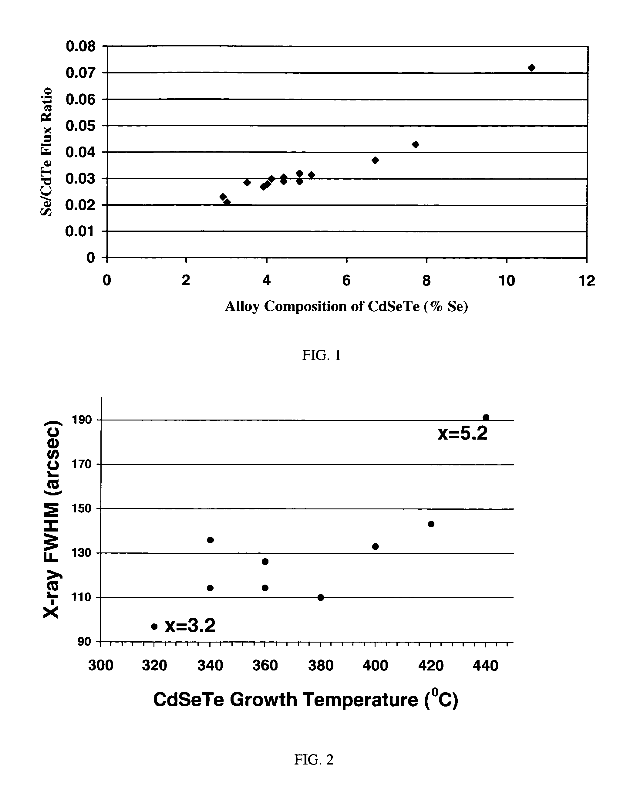
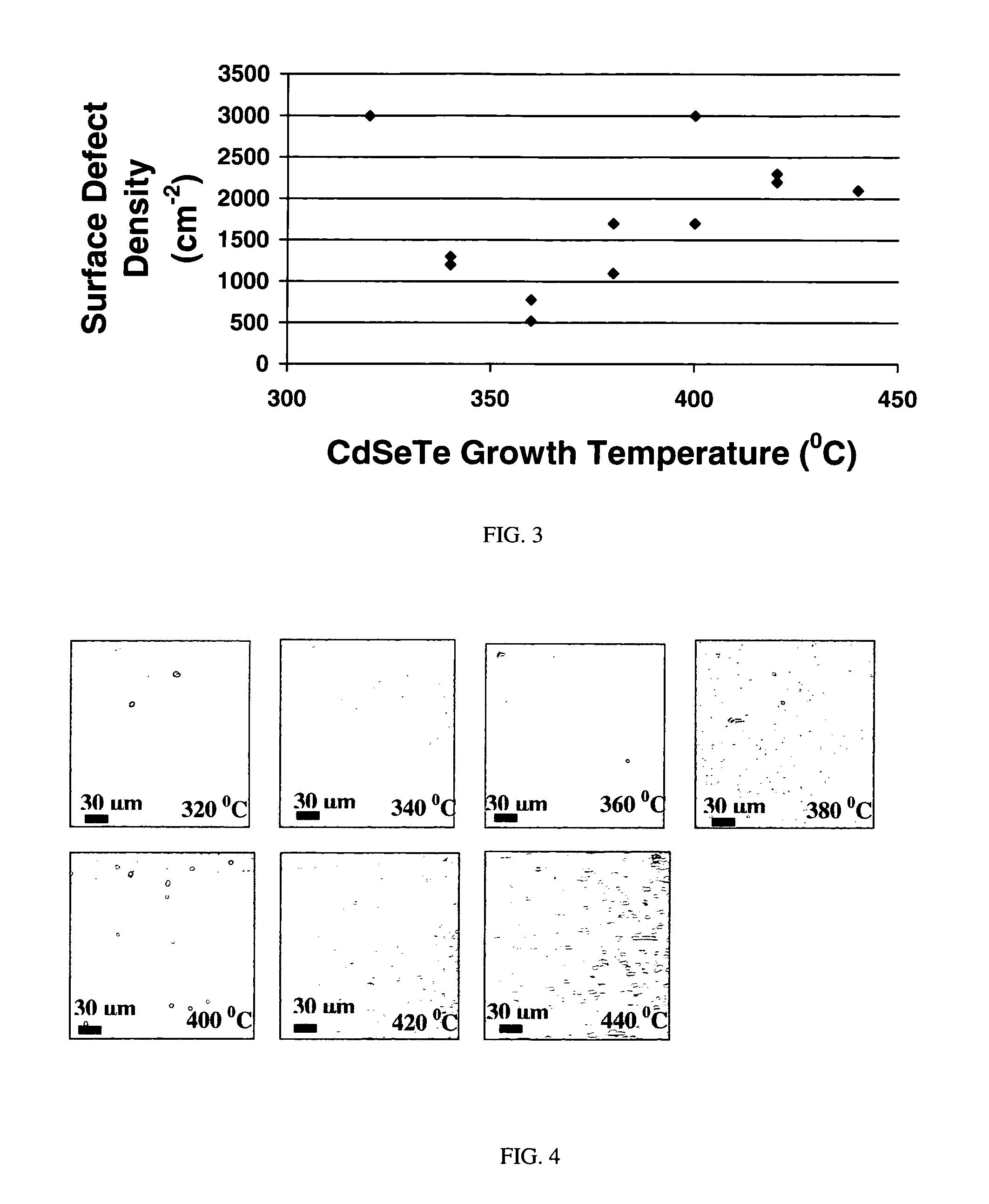
[0027]As used herein, the stated percentage of a particular chalcogenide atom in a ternary compound having two chalcogenide atomic species such (such as CdSeTe) is determined by the relative numbers of atoms of each chalcogenide species in the compound. For example, CdSe0.05Te0.95 is equivalent to CdSeTe having an atomic stoichiometry of 5% Se or 95% Te and Cd0.99Zn0.01Se0.03Te0.97 is equivalent to CdZnSeTe with 1% of Zn relative to Cd and 3% of Se relative to Te. The term “CdSeTe” or “CdZnSeTe” is used herein to represent compounds having the general formula CdSexTe1-x, where 01-zZnzSe...


PUM

PropertyMeasurementUnit
thicknessaaaaaaaaaa
thicknessaaaaaaaaaa
temperaturesaaaaaaaaaa

Abstract

The ternary alloy CdSexTe1-x(2 1 1) and the quaternary alloy Cd1-zZnzSexTe1-x have been grown on Si(2 1 1) substrates using molecular beam epitaxy (MBE). The growth of CdSeTe is facilitated using a compound CdTe effusion source and a Se effusion source while the growth of CdZnSeTe is facilitated using a compound CdTe effusion source, a compound ZnTe effusion source, and an elemental Se source. The alloy compositions (x) and (z) of CdSexTe1-x ternary compound and Cd1-zZnzSexTe1-x are controlled through the Se/CdTe and ZnTe/CdTe flux ratios. The rate of Se incorporation is higher than the rate of Te incorporation as growth temperature increases. As-grown CdSeTe with 4% Se and CdZnSeTe with 4% Zn+Se, which is substantially lattice matched to long-wavelength infrared HgCdTe materials, exhibits excellent surface morphology, low surface defect density (less than 500 cm2), and a narrow X-ray rocking curve (a full-width at half maximum of 103 arcsec).

Description

GOVERNMENT INTEREST[0001]The invention described herein may be manufactured, used, and licensed by or for the United States Government.FIELD OF THE INVENTION[0002]The present invention generally relates to the growth of CdSexTe1-x and Cd1-zZnzSexTe1-x and in particular to the epitaxial growth of CdSexTe1-x and Cd1-zZnzSexTe1-x on silicon.BACKGROUND OF THE INVENTION[0003]For over a decade, the HgCdTe research community has spent considerable effort to prepare CdTe / Si composite substrates for HgCdTe material growth and subsequent infrared (IR) device applications. These research efforts have led to a relatively mature process for CdTe / Si fabrication by MBE. CdTe / Si composite substrates have been used to fabricate large-format short wavelength infrared (SWIR, 1-3 μm) and medium wavelength infrared (MWIR, 3-5 μm) HgCdTe focal plane arrays, despite the lattice mismatch between CdTe and HgCdTe.[0004]However, to advance this technology to long wavelength (LWIR, 8-12 μm) HgCdTe devices, lat...

Claims


Application Information

Patent Timeline
Patent Type & Authority Patents(United States)
IPC IPC(8): H01L31/00
CPCH01L21/02381H01L21/02433H01L21/0256H01L21/02562H01L21/02609H01L21/02631H01L31/02966H01L31/1832H01L31/1836Y02E10/50
Inventor CHEN, YUANPINGBRILL, GREGORYDHAR, NIBIR K.
Owner UNITED STATES OF AMERICA THE AS REPRESENTED BY THE SEC OF THE ARMY
Why Eureka
Try Eureka