Fabrication method of semiconductor integrated circuit device

a technology of integrated circuit device and fabrication method, which is applied in the direction of semiconductor/solid-state device testing/measurement, semiconductor/solid-state device details, instruments, etc., can solve the problems of difficult alignment of probes with disposed positions of test pads, membrane probes may be broken, so as to prevent the breakage of membrane probes

Inactive Publication Date: 2009-06-09
RENESAS ELECTRONICS CORP
View PDF28 Cites 18 Cited by
  • Summary
  • Abstract
  • Description
  • Claims
  • Application Information

AI Technical Summary

Benefits of technology

[0012]Maltifunctionality of a semiconductor integrated circuit device has made much progress in recent years, and elaboration of a plurality of circuits in one semiconductor chip (hereinafter, simply mentioned as chip) is promoted. Moreover, to decrease fabrication cost of the semiconductor integrated circuit device, it is promoted that a semiconductor element and a wiring line are reduced in size so that area of a semiconductor chip (hereinafter simply referred to chip) is reduced, consequently the number of obtained chips per wafer is increased. Therefore, the number of test pads (bonding pads) is increased, in addition, a pitch in arrangement of the test pads is reduced, and area of the test pad is also reduced. In association with such reduction in pitch of the test pads, there is a problem that when a prober having cantilever-like probes is used for the probe test, the probes are hard to be set in alignment with disposed positions of the test pads.
[0016]An object of an invention disclosed in the application is to provide a technique for preventing breakage of the membrane probe in the probe test performed using the probe card having the membrane probe.

Problems solved by technology

In association with such reduction in pitch of the test pads, there is a problem that when a prober having cantilever-like probes is used for the probe test, the probes are hard to be set in alignment with disposed positions of the test pads.
In the case of using such a probe card, if a foreign substance is adhered on a surface of a chip as a test object, the foreign substance may be touched to the membrane probe when a probe is contacted to a test pad, consequently the membrane probe may be broken.
Moreover, in the case that abnormality occurs in shape of the test pad, the membrane probe may be broken.
There is a problem that when the membrane probe is broken in this way, the probe test may be continued while breakage is not noticed, consequently an accurate test result is not obtained.

Method used


Image

  • Fabrication method of semiconductor integrated circuit device
  • Fabrication method of semiconductor integrated circuit device
  • Fabrication method of semiconductor integrated circuit device

Examples


embodiment 1

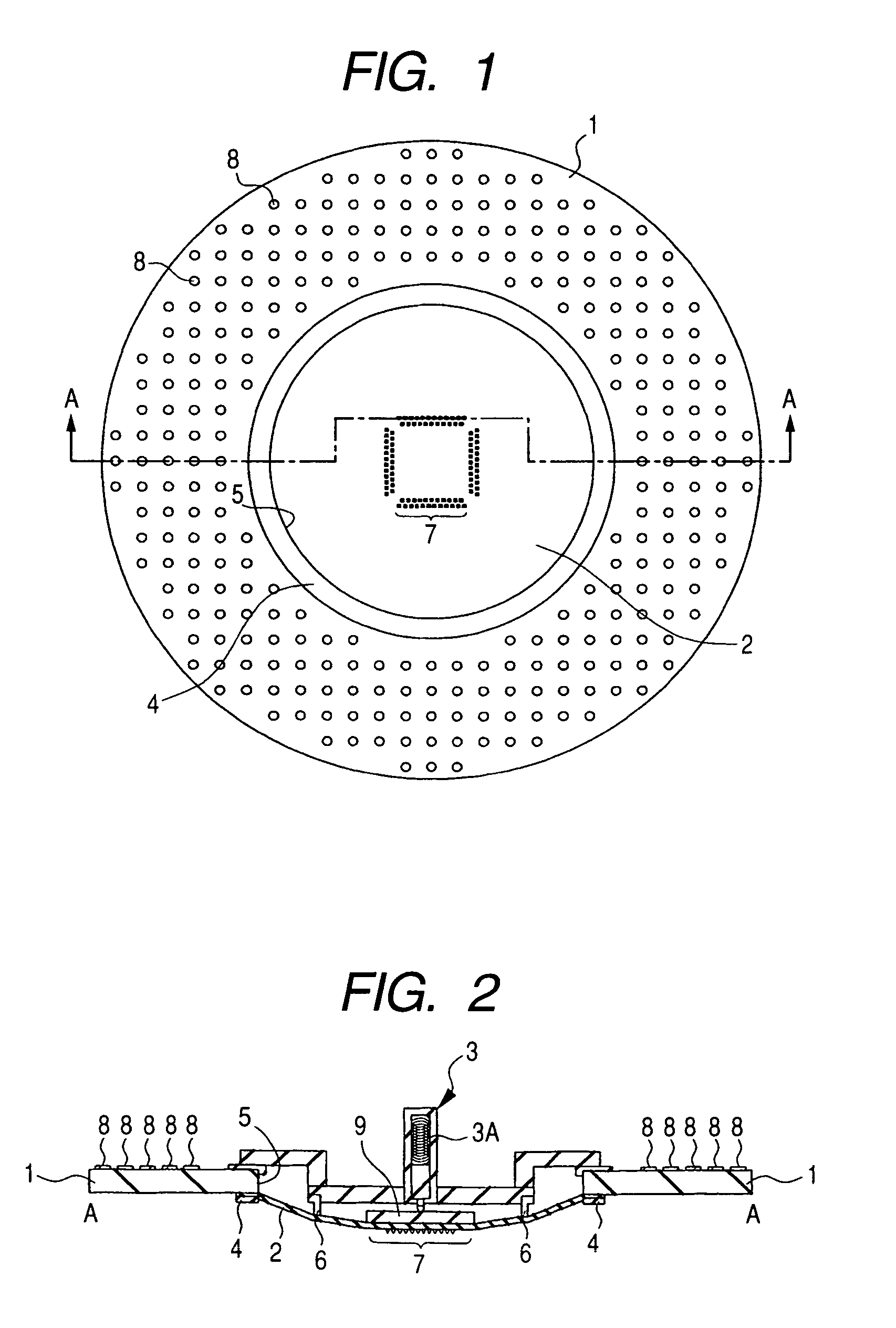
[0165]FIG. 1 shows a relevant-part plane view of a bottom of a probe card of embodiment 1, and FIG. 2 is a cross section view along a line A-A in FIG. 1.

[0166]As shown in FIGS. 1 and 2, the probe card (first card) of the embodiment 1 is formed by a multilayer wiring board 1, membrane sheet (membrane probe (first sheet)) 2, and plunger (pressing mechanism) 3 and the like. The membrane sheet 2 is fixed to a bottom of the multilayer wiring board 1 by a holding ring 4, and the plunger 3 is attached to a top of the multilayer wiring board 1. An opening 5 is provided in the center of the multilayer wiring board 1, in which the membrane sheet 2 and the plunger 3 are adhered to each other via an adhesion ring 6.

[0167]On a bottom of the membrane sheet 2, a plurality of probes (contact terminals) 7 in a form of, for example, quadrangular pyramid or quadrangular pyramid trapezoid are formed. A plurality of wiring lines are formed in the membrane sheet 2, each of the wiring lines being electric...

embodiment 2

[0206]Next, embodiment 2 is described.

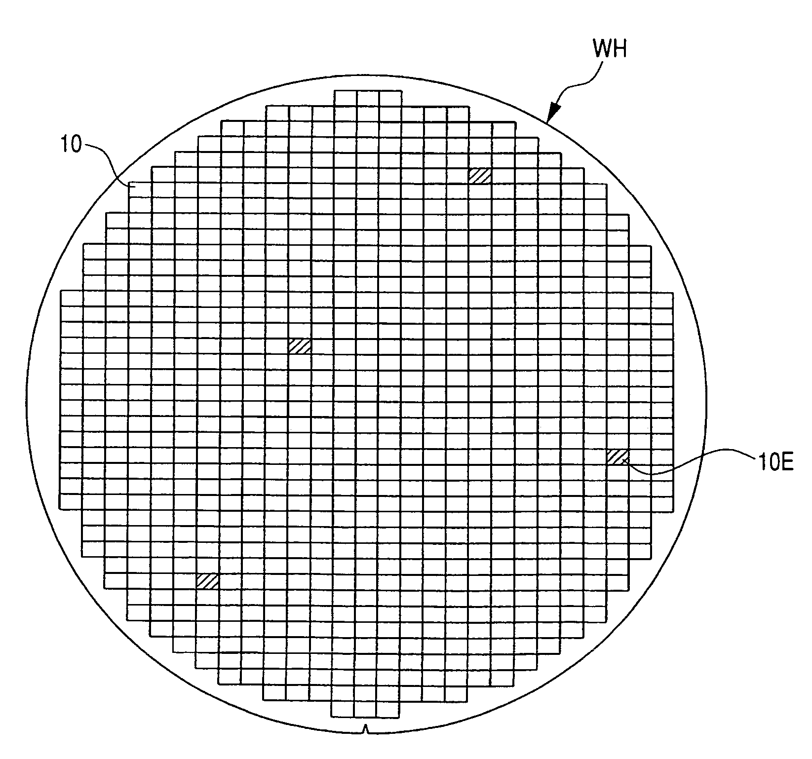
[0207]FIGS. 43 and 44 show relevant-part section views of a chip 10 having an LCD driver formed therein, which was described also in the embodiment 1, and show cross sections different from each other.

[0208]A substrate 61 (wafer WH) includes a p-type single-crystal Si, and in a device formation surface as a main surface of the substrate, an isolation part 62 is formed to define active regions La and dummy active regions Lb. The isolation part 62 includes a silicon oxide film formed by, for example, a LOCOS (Local Oxidation of Silicon) process. However, the isolation part 62 may be formed by an isolation part 62 in a groove type (SGI: Shallow Groove Isolation or STI: Shallow Trench Isolation).

[0209]For example, a pn-junction diode D is formed in an active region La enclosed by the isolation part 62 in the substrate 61 as a layer under a pad PD1 as shown in FIG. 43. The pn-junction diode D is, for example, a protective diode for preventing electro...

embodiment 3

[0216]FIG. 47 shows a cross section view showing a relevant part of a semiconductor chip in which a semiconductor integrated circuit device of embodiment 3 is formed, wherein a section at the left on paper shows a region where a stacked wiring is formed, and a section at the right on paper shows a region where a bonding pad (hereinafter, simply refer to pad) is formed.

[0217]A p-type well 82 is formed over a main surface of a substrate 81 including p-type single crystal Si (silicon), and an element isolation groove 83 is formed in an element isolation region of the p-type well. The element isolation groove 83 is in a configuration where a groove formed by etching the substrate 81 is filled with an insulating film 84 such as a silicon oxide film.

[0218]N-channel type MISFET Qn mainly includes a gate oxide film 85, gate electrode 6, and n-type semiconductor regions (source, drain) 87 in an LDD (Lightly Doped Drain) structure. The gate electrode 6 is formed by a 3-layer conductive film f...


PUM


Abstract

To prevent breakage of a membrane probe during a probe test using a probe card having the membrane probe, appearance of a main surface of a wafer as a test object is tested by an appearance tester 51, and results of bad appearance such as adhesion of a foreign substance to the main surface of the wafer and abnormality in shape of bump electrodes over the main surface of the wafer are collected as wafer map data according to arrangement of respective chips in a plane of the wafer, then the wafer map data are transmitted to a probe tester 53 via a server 52, and the probe tester 53 omits the probe test for chips in which bad appearance was detected, and concurrently performs the probe test to other chips in which bad appearance was not detected, based on the wafer map data.

Description

TECHNICAL FIELD[0001]The present invention relates to a technique of fabricating a semiconductor integrated circuit device, and particularly relates to a technique effectively used for an electric test of a semiconductor integrated circuit on which a number of electrode pads are disposed at a narrow pitch.BACKGROUND ART[0002]For example, Japanese Patent Laid-open Nos. 7-283280, 8-50146 (corresponding to international publication WO 95 / 34000), 8-201427, 11-23615 (corresponding to U.S. Pat. No. 6,305,230), 2001-159643, 10-308423, 11-97471 (corresponding to European Patent No. EP 1022775), and 2000-150594 (corresponding to European Patent No. EP 0999451) disclose a structure of a prober having a probe (contact terminal) formed using a technique of fabricating a semiconductor integrated circuit device, an insulating film, and lead lines, a method of fabricating the prober, and a technique of enabling practice of a probe test even for a chip having test pads with a reduced pitch by using...

Claims


Application Information

Patent Timeline
Patent Type & Authority Patents(United States)
IPC IPC(8): H01L21/66G01R31/28H01L23/485
CPCG01R31/2894H01L22/20H01L24/06H01L24/05H01L24/13H01L2924/1306H01L2224/0231H01L2224/0401H01L2224/05553H01L2224/13099H01L2924/01005H01L2924/01006H01L2924/01013H01L2924/01014H01L2924/01015H01L2924/01022H01L2924/01027H01L2924/01028H01L2924/01029H01L2924/01033H01L2924/01046H01L2924/01047H01L2924/0105H01L2924/01057H01L2924/01074H01L2924/01078H01L2924/01079H01L2924/01082H01L2924/014H01L2924/04941H01L2924/05042H01L2924/13091H01L2924/14H01L2924/01019H01L2924/01024H01L2924/01045H01L2224/05085H01L2924/00H01L2224/0392H01L2924/12036H01L2924/12041H01L2924/15788
Inventor KANDA, MAKOTOWATANABE, KOJIHIROTA, DAISUKE
Owner RENESAS ELECTRONICS CORP
Why Eureka
Try Eureka