Method of manufacturing nitride-based semiconductor light emitting diode

a technology of light-emitting diodes and nitride, which is applied in the direction of semiconductor devices, basic electric elements, electrical equipment, etc., can solve the problems of poor layer quality, low hole concentration, and difficulty in forming ohmic contact with an electrode, so as to improve the activation process of a p-type nitride semiconductor layer, reduce contact resistance, and increase the hole concentration

Inactive Publication Date: 2009-08-18
SAMSUNG ELECTRONICS CO LTD
View PDF21 Cites 0 Cited by
  • Summary
  • Abstract
  • Description
  • Claims
  • Application Information

AI Technical Summary

Benefits of technology

[0019]An advantage of the present invention is that it provides a method of manufacturing a nitride semiconductor LED, which can improve an activation process of a p-type nitride semiconductor layer to increase hole concentration within the p-type nitride semiconductor layer, reduce contact resistance to implement a low operation voltage, and enhance internal quantum efficiency.
[0020]Additional aspect and advantages of the present general inventive concept will be set forth in part in the description which follows and, in part, will be obvious from the description, or may be learned by practice of the general inventive concept.
[0021]According to an aspect of the invention, a method of manufacturing a nitride-based semiconductor LED comprises sequentially forming an n-type nitride semiconductor layer, an active layer, and a p-type nitride semiconductor layer on a substrate; forming a Pd / Zn alloy layer on the p-type nitride semiconductor layer; heat-treating the p-type nitride semiconductor layer on which the Pd / Zn alloy layer is formed; removing the Pd / Zn alloy layer formed on the p-type nitride semiconductor layer; mesa-etching portions of the p-type nitride semiconductor layer, the active layer, and the n-type nitride semiconductor layer such that a portion of the upper surface of the n-type nitride semiconductor layer is exposed; and forming an n-electrode and a p-electrode on the exposed n-type nitride semiconductor layer and the p-type nitride semiconductor layer, respectively.
[0022]Preferably, the Pd / Zn alloy layer is formed on the p-type nitride semiconductor layer excluding the region where the p-electrode is formed.
[0023]Preferably, the removing of the Pd / Zn alloy layer is performed in such a manner that the concentration of Pd and Zn remaining in the p-type nitride semiconductor layer is maintained at 1×10¹⁶ to 1×1020 cm−3, through the heat-treating of the p-type nitride semiconductor layer. Further, Pd and Zn remaining in the p-type nitride semiconductor layer are positioned in the range of 2 to 100 nm from the upper surface of the p-type nitride semiconductor layer.
[0024]Preferably, the removing of the Pd / Zn alloy layer is performed in such a manner that the surface roughness of the p-type nitride semiconductor layer coming in contact with the Pd / Zn alloy layer is maintained at 0.5 to 10 nm.

Problems solved by technology

However, since such a nitride-based semiconductor has a relatively large energy band-gap, there are difficulties in forming the ohmic contact with an electrode.
However, when the p-type nitride semiconductor layer 140 is grown, p-type Mg elements serving as doping elements are used as dopants like the n-type nitride semiconductor layer 120, but a layer quality is bad and hole concentration is low because of the following three main factors.
Therefore, it is difficult to implement a p-type nitride semiconductor layer with high concentration.
However, the activation ratio is still low.

Method used


Image

  • Method of manufacturing nitride-based semiconductor light emitting diode
  • Method of manufacturing nitride-based semiconductor light emitting diode
  • Method of manufacturing nitride-based semiconductor light emitting diode

Examples


first embodiment

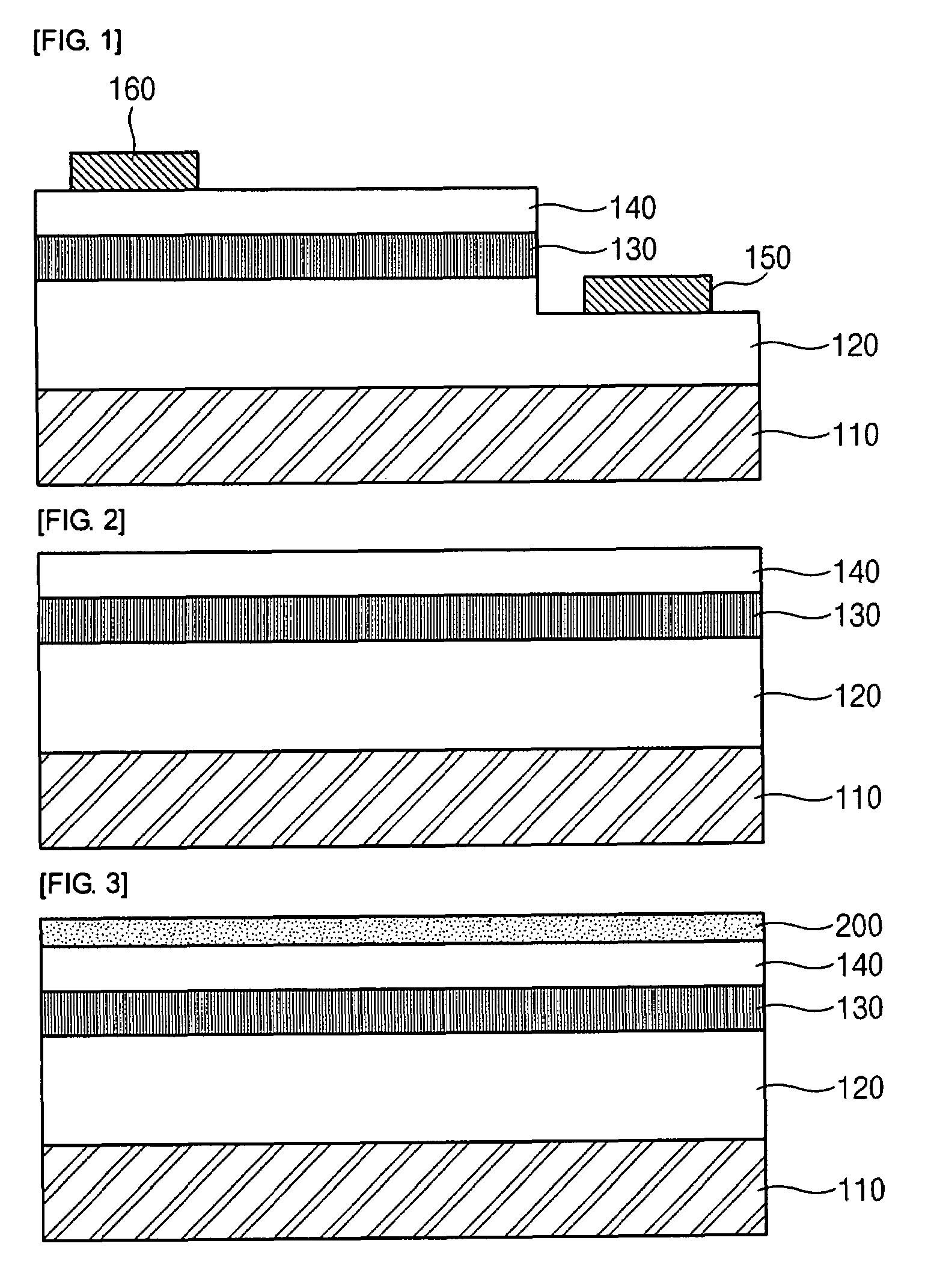
[0036]FIGS. 2 to 7 are sectional views sequentially showing a process for explaining a method of manufacturing a nitride-based semiconductor LED according to a first embodiment of the invention.

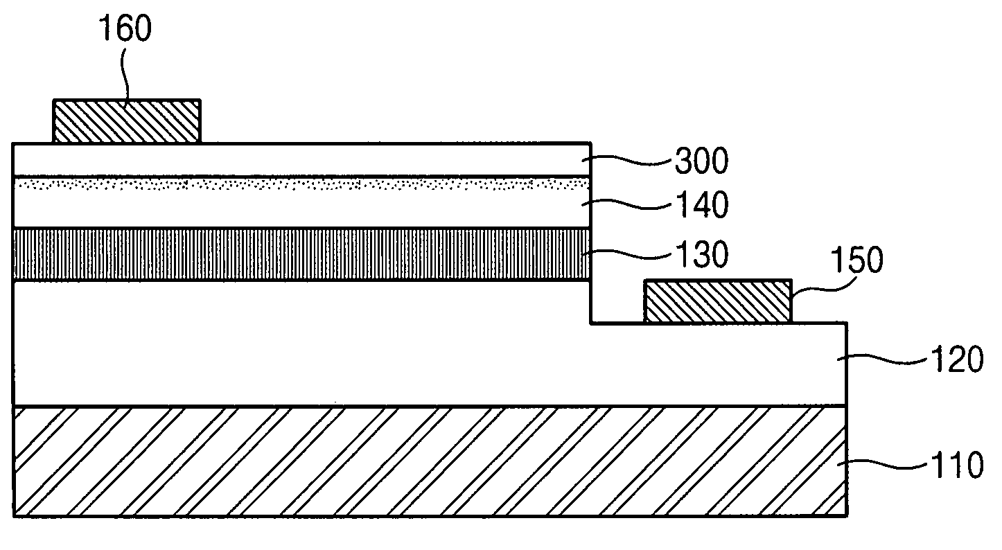
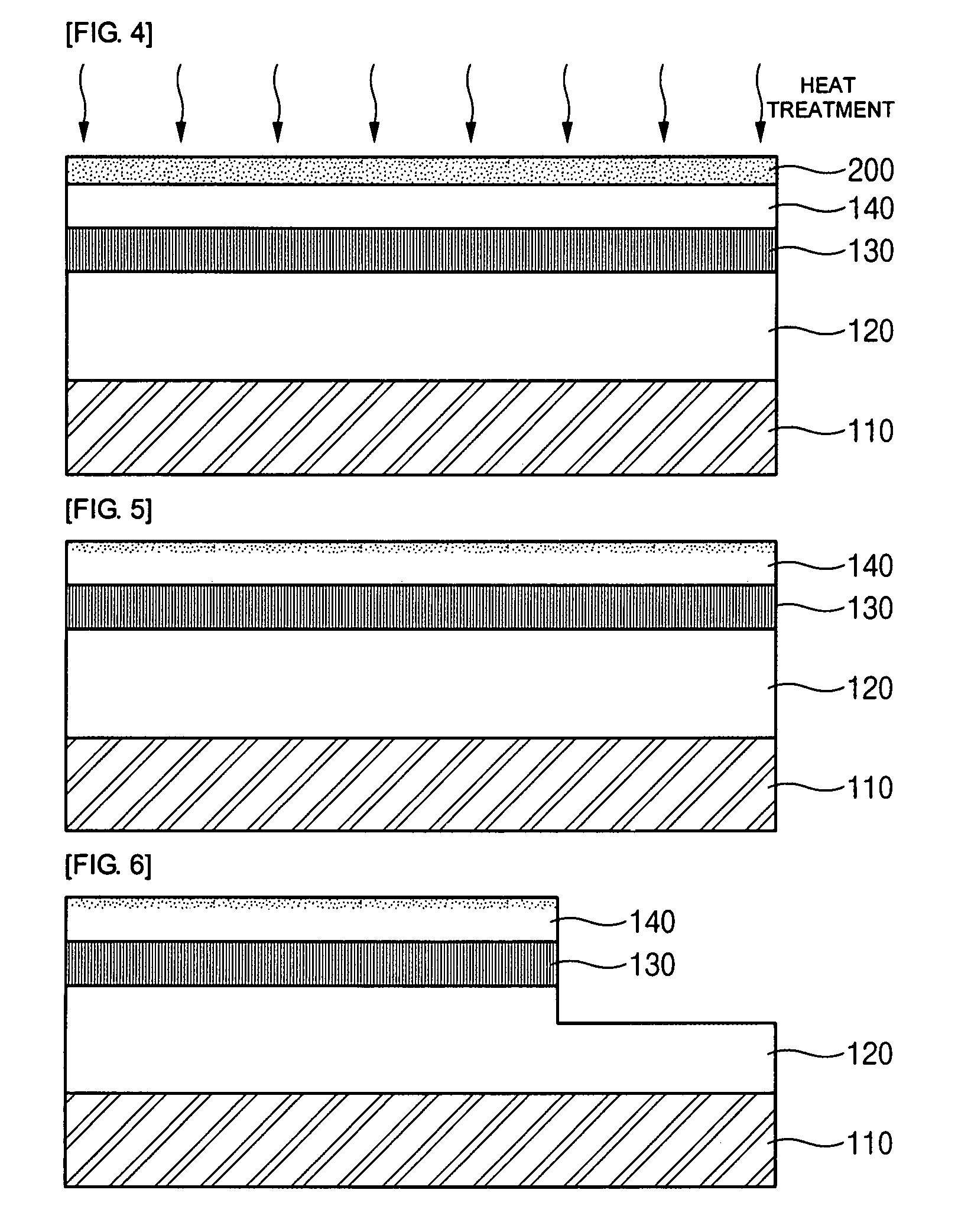
[0037]First, as shown in FIG. 2, an n-type nitride semiconductor layer 120, a GaN / InGaN active layer 130 with a multi-quantum well structure, and a p-type nitride semiconductor layer 140 are sequentially laminated on a substrate 110, thereby forming a light emission structure.

[0038]Preferably, the substrate 110 is formed of a transparent material containing sapphire. In addition to sapphire, the substrate 100 may be formed of zinc oxide (ZnO), gallium nitride (GaN), silicon carbide (SiC), or aluminum nitride (AlN).

[0039]Although not shown, a GaN-based or SiC-based buffer layer for enhancing the lattice matching between the substrate 100 and the n-type nitride semiconductor layer 120 is further formed before the n-type nitride semiconductor layer 120 is formed on the substrate 110. The buffer ...

second embodiment

[0054]Referring to FIG. 9, a method of manufacturing a nitride-based semiconductor LED according to a second embodiment of the invention will be described. However, the descriptions of the same components as those of the first embodiment will be omitted.

[0055]FIG. 9 is a cross-sectional view of a nitride-based semiconductor LED manufactured according to a second embodiment of the invention.

[0056]As shown in FIG. 9, the nitride-based semiconductor LED manufactured according to the second embodiment has almost the same construction as that of the nitride-based semiconductor LED manufactured according to the first embodiment. However, the nitride-based semiconductor LED manufactured according to the second embodiment is different from the nitride-based semiconductor LED manufactured according to the first embodiment only in that the Pd / Zn alloy layer 200 at the interface between the p-type nitride semiconductor layer 140 and the p-electrode 160 is not removed but remains.

[0057]That is,...


PUM

PropertyMeasurementUnit
surface roughnessaaaaaaaaaa
energy band gapaaaaaaaaaa
electron concentrationaaaaaaaaaa

Abstract

Provided is a method of manufacturing a nitride-based semiconductor LED including sequentially forming an n-type nitride semiconductor layer, an active layer, and a p-type nitride semiconductor layer on a substrate; forming a Pd / Zn alloy layer on the p-type nitride semiconductor layer; heat-treating the p-type nitride semiconductor layer on which the Pd / Zn alloy layer is formed; removing the Pd / Zn alloy layer formed on the p-type nitride semiconductor layer; mesa-etching portions of the p-type nitride semiconductor layer, the active layer, and the n-type nitride semiconductor layer such that a portion of the upper surface of the n-type nitride semiconductor layer is exposed; and forming an n-electrode and a p-electrode on the exposed n-type nitride semiconductor layer and the p-type nitride semiconductor layer, respectively.

Description

CROSS-REFERENCE TO RELATED APPLICATIONS[0001]This application claims the benefit of Korean Patent Application No. 10-2007-0049633 filed with the Korean Intellectual Property Office on May 22, 2007, the disclosure of which is incorporated herein by reference.BACKGROUND OF THE INVENTION[0002]1. Field of the Invention[0003]The present invention relates to a method of manufacturing a nitride-based semiconductor light emitting diode (LED), which can implement a low operation voltage and enhance internal quantum efficiency.[0004]2. Description of the Related Art[0005]In general, a nitride-based semiconductor is such a material that has a relatively high energy band gap (in the case of GaN semiconductor, about 3.4 eV), and is positively adopted in an optical device for generating green or blue short-wavelength light. As for the nitride semiconductor, a material having a compositional formula of AlxInyGa(1-x-y)N (herein, 0≦x≦1, 0≦y≦1, and 0≦x+y≦1) is widely used.[0006]However, since such a ...

Claims


Application Information

Patent Timeline
Patent Type & Authority Patents(United States)
IPC IPC(8): H01L21/4763H01L33/32H01L33/40H01L33/42
CPCH01L33/40H01L33/32H01L33/42
Inventor KIM, SUN WOONPARK, SEONG JUKIM, JA YEONKWON, MIN KILEE, DONG JUHAN, JAE HO
Owner SAMSUNG ELECTRONICS CO LTD
Why Eureka
Try Eureka