Method for exposing photo-sensitive SAM film and method for manufacturing semiconductor device

a technology of photosensitive sam film and manufacturing method, which is applied in the direction of photomechanical equipment, photosensitive material processing, instruments, etc., can solve the problems of increased manufacturing cost, inability to fabricate fine tft by printing process, and inability to meet the requirements of the respective processes and apparatuses, etc., to achieve accurate alignment

Inactive Publication Date: 2009-09-08
HITACHI LTD
View PDF5 Cites 4 Cited by
  • Summary
  • Abstract
  • Description
  • Claims
  • Application Information

AI Technical Summary

Benefits of technology

[0007]As described above, a TFT manufacturing method using a printing technology has a feature that the price reduction can be achieved. In a current general printing technology, however, its alignment accuracy is about 10 μm, and even if the latest technology is used, it is about several μm. Therefore, it is difficult to fabricate a fine TFT by the printing process. In particular, when misalignment occurs between a gate electrode (lower electrode) and a source / drain electrode (upper electrode), a parasitic capacity is increased or performance variation is caused in the case where a plurality of TFTs are fabricated. It is said that this misalignment occurs at the time when the material jetted from a nozzle flies to a substrate in the ink-jet method. Also, it is said that it occurs at the time when the material is transferred from a transferring roller to a substrate in the transfer method.
[0011]For the problems described above, an object of the present invention is to provide a method for manufacturing a high-performance organic thin film transistor including electrodes having fine pattern shapes of about 20 μm formed in a short time by using a printing method, in which a lower electrode and an upper electrode aligned to suppress a misalignment therebetween of 1 μm or less without using a photomask face each other via an insulating film.
[0017]A representative embodiment of the present invention uses a manufacturing method in which a process for forming a source and drain electrode material by the use of a difference in the contact angle of water or organic solvent varied by the exposure without using a mask is used only for the process of alignment between the upper electrode and the lower electrode, and a printing method is used for all the other processes. A translucent substrate is prepared and a conductive material is printed and burned on the translucent substrate, thereby fabricating a non-translucent gate electrode (lower electrode). On the non-translucent gate electrode, a translucent insulating film and a photo-sensitive self-assembled-monolayer solution on which the contact angle of water or an organic solution varies by the exposure are sequentially stacked in required areas by the printing method. Then, while the substrate is dipped in alkaline aqueous solution or organic solvent or while a surface (surface on which the photo-sensitive self-assembled-monolayer is formed) of the substrate is brought into contact with alkaline aqueous solution or organic solvent, the photo-sensitive self-assembled-monolayer is exposed from the rear surface of the substrate with using the lower electrode as a mask. Thereafter, the substrate is rinsed with water to increase a difference in the contact angle of water or organic solvent between an exposed portion and an unexposed portion, and the conductive material solution is printed by the use of the difference, so that source and drain electrode patterns aligned with the lower electrode can be formed. In this manner, the accurate alignment between the lower electrode and the upper electrode can be achieved. Thereafter, an organic semiconductor material is printed or deposited just above the lower electrode, thereby forming an organic thin film transistor.
[0018]According to the embodiments of the present invention, it is possible to provide a semiconductor device including an organic thin film transistor having electrodes in which a lower electrode and an upper electrode accurately aligned by using a printing method within 1 μm face each other via an insulating film.

Problems solved by technology

Therefore, it is difficult to fabricate a fine TFT by the printing process.
In this case, since both the processes are used in combination, fabrication apparatuses such as a photolithography related apparatus, a printer, a film forming apparatus, and an etching apparatus are wide-ranging and complicated, and a manufacturing cost increases because photomasks are required for the contact hole formation process, the electrode formation process, and the like.
Although the pattern formation without causing misalignment is possible by using this method, since the photo-sensitive composition photolithography process is performed and such processes as photo-sensitive composition application, heating, exposure, and development are included therein, extra cost and time are required for the respective processes and apparatuses to be used.
Further, when the photo-sensitive composition photolithography process used in the common semiconductor process is used, there is a possibility that a special substrate such as a flexible substrate cannot be used.
Further, when an organic type material such as plastic is used for a substrate, a problem occurs in which the substrate is dissolved in a photo-sensitive composition solvent.
However, since an irradiation dose of about ten times as large as that in the common resist photolithography process is required so far in order to develop the hydrophilic property of the photo-sensitive SAM, there is a problem that much time is required.

Method used


Image

  • Method for exposing photo-sensitive SAM film and method for manufacturing semiconductor device
  • Method for exposing photo-sensitive SAM film and method for manufacturing semiconductor device
  • Method for exposing photo-sensitive SAM film and method for manufacturing semiconductor device

Examples


first embodiment

[0089]A photo-sensitive SAM film is formed on a silicon wafer by dipping the silicon wafer in 0.1 w % toluene solution of a photo-sensitive self-assembled-monolayer material (5-methoxy-2-nitro-benzyl 4-(trimethoxysilyl)butanesulfonate) for 20 minutes. The contact angle of water of the surface of the substrate at this time is 95°. Three pieces of such substrates are prepared, and one of them is exposed in the atmosphere and the other two substrates are respectively exposed in toluene and in tetramethylammonium hydroxide (TMAH) 2.38 w % aqueous solution in the exposure system shown in FIG. 23 with using a high pressure mercury lamp as a light source.

[0090]As a result, in order to decrease the contact angle completely, an irradiation dose of 40 J / cm2 is required in the atmosphere. Further, it is found that, in the exposure in toluene and TMAH, the contact angle settles at 20° by an irradiation dose of 6 J / cm2 which is about one-sixth of the irradiation dose in the exposure in the atmos...

second embodiment

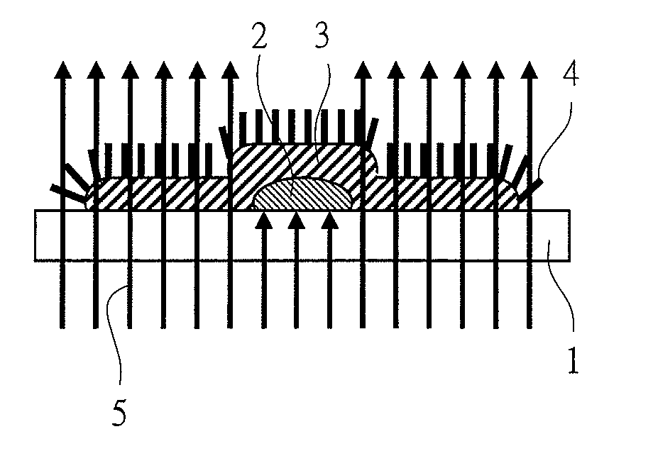
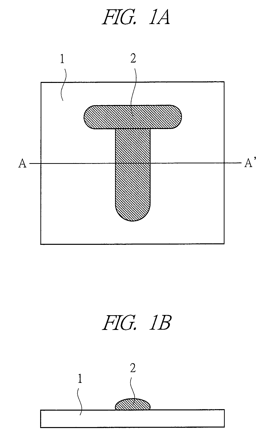
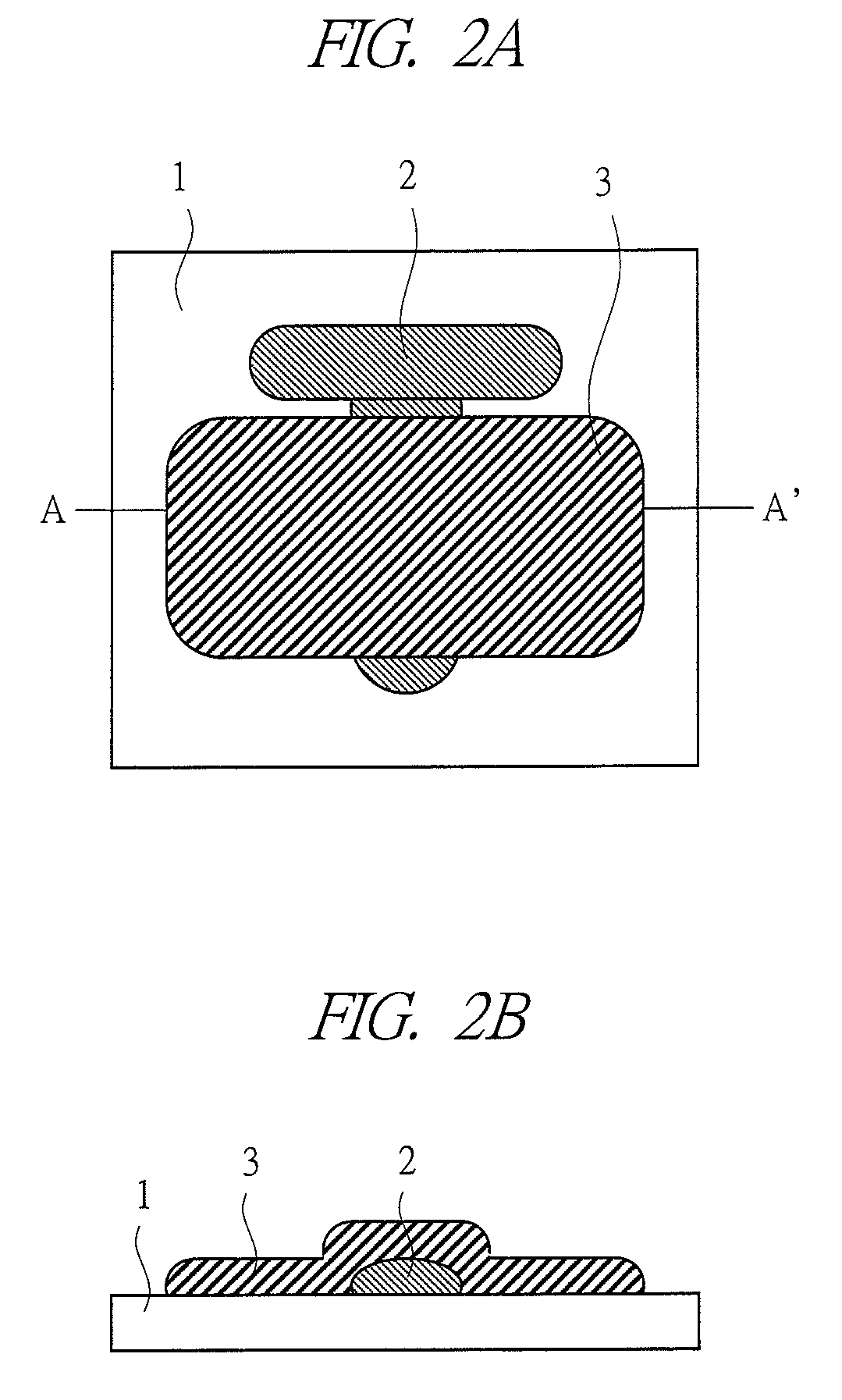
[0092]FIG. 1A to FIG. 8B are plan views and sectional views of a device shown in order of manufacturing steps of this embodiment in which source and drain electrodes are formed by exposure from the rear surface of the substrate. FIG. 1A to FIG. 8A are top views, and FIG. 1B to FIG. 8B are sectional views taken along the line A-A′ in respective FIG. 1A to FIG. 8A. In the top views and the sectional views of the device shown in order of the manufacturing steps in the specification of this application, FIG. 1A to FIG. 8A show top views and FIG. 1B to FIG. 8B show sectional views.

[0093]Polycarbonate which is an organic compound is used as a translucent substrate 1, and a gate electrode shape with a line width of 20 μm is printed on the substrate 1 by the ink-jet printing method with using gold nanoparticles dispersed in toluene solution as ink. Then, the substrate 1 is heated for 5 minutes at 200° C., thereby forming a gold gate electrode 2 (top view: FIG. 1A, sectional view: FIG. 1B). ...

third embodiment

[0100]This embodiment describes an example in which two organic semiconductor transistors (19, 20) are formed by the same method as that used in the second embodiment. A top view and a sectional view of this embodiment are shown in FIG. 9 and FIG. 10. A method for forming the respective transistors is similar to that used in the above-described first embodiment, but in the configuration of this embodiment, after the respective transistors are formed, a drain electrode 6 of a first transistor 19 of the transistors and a second gate electrode 2 of the other transistor 20 are connected to each other through a wiring 11. FIG. 9 shows the top view and FIG. 10 shows the sectional view taken along the line A-A′ in FIG. 9. Performances of both the transistors are exactly the same, and the transistors having no performance variation can be fabricated.

[0101]In the second and the third embodiments, representative examples which are especially high-quality in both cost and performance have been...


PUM

PropertyMeasurementUnit
exposure-wavelengthaaaaaaaaaa
temperatureaaaaaaaaaa
heatproof temperatureaaaaaaaaaa

Abstract

A disclosed technology is a method for exposing a photo-sensitive SAM film, wherein a self-assembled-monolayer (photo-sensitive SAM film) having photo-sensitivity, exhibiting hydrophobicity before exposure, and exhibiting hydrophilicity after exposure is formed on a substrate, exposure is performed to the substrate in a state in which a surface of the substrate on which the film has been formed is dipped in liquid or in a state in which a light-sensitive surface of the substrate faces downward to be in contact with liquid, exposure light is ultraviolet light, visible light, or light with an exposure-wavelength of 350 nm or more to 800 nm or less, and the liquid is at least one of organic solvent containing an aromatic group and organic solvent of alcohols, ethers, or ketones.

Description

CROSS-REFERENCE TO RELATED APPLICATION[0001]The present application claims priority from Japanese Patent Application No. JP 2007-117955 filed on Apr. 27, 2007, the content of which is hereby incorporated by reference into this application.TECHNICAL FIELD OF THE INVENTION[0002]The present invention relates to a method for exposing a photo-sensitive SAM film and a method for manufacturing a semiconductor device. More particularly, it relates to a method for manufacturing a semiconductor device including an organic thin film transistor, a method for exposing a self-assembled-monolayer film having photo-sensitivity, an organic thin film transistor using the self-assembled-monolayer film and a method for manufacturing the organic thin film transistor, and a semiconductor device including an organic thin film transistor and a method for manufacturing the semiconductor device.BACKGROUND OF THE INVENTION[0003]In recent years, various research and development of a display device including a ...

Claims


Application Information

Patent Timeline
Patent Type & Authority Patents(United States)
IPC IPC(8): H01L21/00G03F7/16G03F7/20G03F7/40
CPCG03F7/165H01L51/102H01L51/0023H01L51/055Y10S977/901Y10S977/896H10K71/621H10K10/481H10K10/82
Inventor ARAI, TADASHISHIBA, TAKEOANDO, MASAHIKO
Owner HITACHI LTD
Why Eureka
Try Eureka