
Semiconductor device

a technology of semiconductor devices and semiconductors, applied in semiconductor devices, semiconductor/solid-state device details, electrical apparatus, etc., can solve the problems of reducing the drain current, increasing the contact resistance, and reducing the device characteristics, so as to suppress the electric field concentration, promote heat diffusion, and improve the breakdown voltage of the fet

Active Publication Date: 2010-02-02
PANASONIC CORP
View PDF8 Cites 14 Cited by
  • Summary
  • Abstract
  • Description
  • Claims
  • Application Information

AI Technical Summary

Benefits of technology

"The present invention aims to improve heat dissipation from semiconductor devices and allow for high-power operations. To achieve this, a passivation film is formed on the semiconductor layer and electrodes using a deposited film consisting of at least two layers having different compositions. Aluminum nitride is used as one of the layers, which has higher thermal conductivity than silicon nitride, to efficiently dissipate heat. The passivation film includes a first sub-film made of aluminum nitride and a second sub-film made of silicon nitride to prevent degradation from ambient moisture and improve high-frequency characteristics. The semiconductor layer is made of a Group III nitride semiconductor and the electrodes can be a gate electrode, source electrode, and drain electrode. The surface of the passivation film is uneven to increase heat dissipation. A heat dissipation film can also be added to further improve heat dissipation."

Problems solved by technology

Such an increase in the device temperature causes degradation in device characteristics, such as a reduction in the drain current.
In addition, when the AlN epitaxial layer is subjected to dry etching, etching damage is caused also to an ohmic electrode formation region, leading to an increase in contact resistance.

Method used


Image

  • Semiconductor device
  • Semiconductor device
  • Semiconductor device

Examples


embodiment 1

[0047]A first embodiment of the present invention will be described with reference to the drawings.

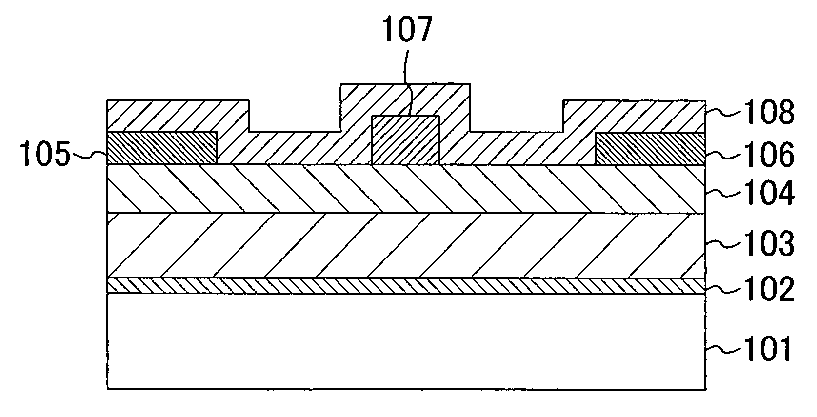
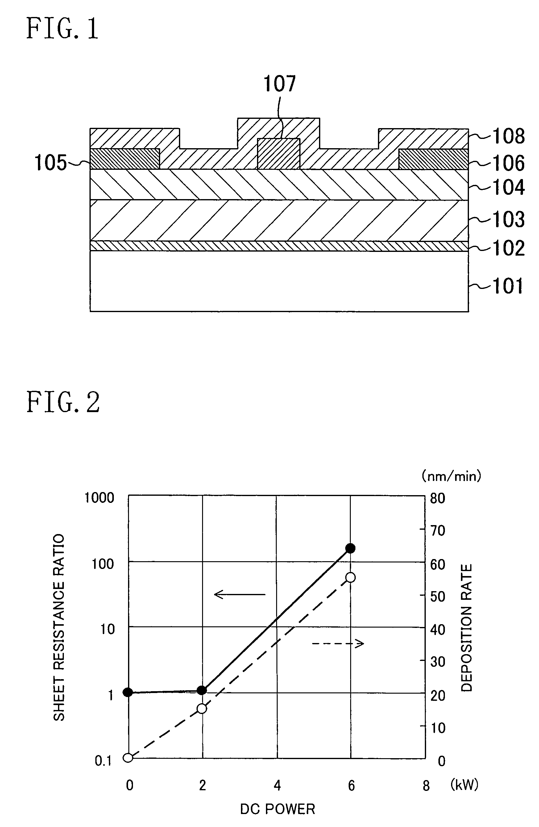
[0048]FIG. 1 illustrates a cross-sectional structure of a semiconductor device according to the first embodiment of the present invention. As illustrated in FIG. 1, a buffer layer 102 made of aluminum nitride (AlN), an underlying layer 103 made of gallium nitride (GaN) and a barrier layer 104 made of Al0.26Ga0.74N are sequentially formed on a substrate 101 made of sapphire (single crystal Al2O3), for example, by metal organic chemical vapor deposition (MOCVD).

[0049]A source electrode 105 and a drain electrode 106 both made of titanium (Ti) and aluminum (Al) are formed on the barrier layer 104 so as to be spaced, and a gate electrode 107 made of an alloy of palladium and silicon (PdSi) is formed between the source electrode 105 and the drain electrode 106, thereby forming a field effect transistor (FET).

[0050]A passivation film 108 made of aluminum nitride (AlN) is deposited, for exampl...

embodiment 2

[0063]A second embodiment of the present invention will be described hereinafter with reference to the drawings.

[0064]FIG. 5 illustrates a cross-sectional structure of a semiconductor device according to the second embodiment of the present invention. In FIG. 5, the same components as those illustrated in FIG. 1 are denoted by the same reference numerals, and thus the description thereof is omitted.

[0065]As illustrated in FIG. 5, the semiconductor device of the second embodiment is configured such that a passivation film 108 is formed of a first sub-film 108a made of aluminum nitride (AlN) and a second sub-film 108b covering the first sub-film 108b and made of silicon nitride (SiN).

[0066]The passivation film 108 of the second embodiment is formed in the following manner: A first sub-film 108a made of AlN is deposited by DC sputtering as in the first embodiment, and then a second sub-film 108b made of SiN is deposited, for example, by plasma CVD to cover the first sub-film 108a.

[006...

embodiment 3

[0071]A third embodiment of the present invention will be described hereinafter with reference to the drawings.

[0072]FIG. 6A illustrates a cross-sectional structure of a semiconductor device according to a third embodiment of the present invention. In FIG. 6A, the same components as those illustrated in FIG. 1 are denoted by the same reference numerals, and thus the description thereof is omitted.

[0073]As illustrated in FIG. 6A, the semiconductor device of the third embodiment is configured such that a passivation film 108 is formed of a second sub-film 108b made of silicon nitride (SiN) and a first sub-film 108a covering the second sub-film 108b and made of aluminum nitride (AlN).

[0074]The passivation film 108 of the third embodiment is formed in the following manner: An approximately 10-nm-thick second sub-film 108b made of SiN is deposited, for example, by plasma CVD to cover a barrier layer 104 and electrodes 105, 106 and 107, and then a first sub-film 108a made of AlN is deposi...


PUM


Abstract

A semiconductor device includes: a semiconductor layer; at least one electrode formed on a semiconductor layer to be in contact with the semiconductor layer; and a passivation film covering the semiconductor layer and at least part of the top surface of the electrode to protect the semiconductor layer and formed of a plurality of sub-films. The passivation film includes a first sub-film made of aluminum nitride.

Description

CROSS-REFERENCE TO RELATED APPLICATIONS[0001]The disclosure of Japanese Patent Application No. 2006-253920 filed on Sep. 20, 2006 including specification, drawings and claims is incorporated herein by reference in its entirety.BACKGROUND OF THE INVENTION[0002](1) Field of the Invention[0003]The present invention relates to semiconductor devices for use in millimeter wave communications or power switching applications.[0004](2) Description of Related Art[0005]Group III nitride semiconductors typified by gallium nitride (GaN) and serving as a mixed crystal material represented by the general formula (InxAl1-x)yGa1-yN (where 0≦x≦1 and 0≦y≦1), have been expected to be applied not only to light-emitting devices for emitting visible or ultraviolet light by utilizing their physical features, i.e., a wide band gap, and a direct transition band structure, but also to electronic devices by utilizing their features, i.e., high breakdown voltage and high saturated electron velocity. Particularl...

Claims


Application Information

Patent Timeline
Patent Type & Authority Patents(United States)
IPC IPC(8): H01L23/58
CPCH01L23/367H01L23/3677H01L29/7787H01L29/2003H01L2924/0002H01L2924/00
Inventor MURATA, TOMOHIROUENO, HIROAKIISHIDA, HIDETOSHIUEDA, TETSUZOUEMOTO, YASUHIROTANAKA, TSUYOSHIUEDA, DAISUKE
Owner PANASONIC CORP
Learn More