Nitride-based semiconductor substrate and method of making the same

a technology of nitride-based semiconductors and substrates, which is applied in the direction of crystal growth process, polycrystalline material growth, natural mineral layered products, etc., can solve the problems of high brightness, failure to manufacture gan-based ld and high brightness, and single crystal film of gan cannot be grown directly on the sapphire substrate. , to achieve the effect of high conductivity and high transparency

Active Publication Date: 2010-02-16
SUMITOMO CHEM CO LTD
View PDF14 Cites 3 Cited by
  • Summary
  • Abstract
  • Description
  • Claims
  • Application Information

AI Technical Summary

Benefits of technology

[0015]It is an object of the invention to provide a nitride-based semiconductor substrate that satisfies a high transparency and a high conductivity together.

Problems solved by technology

However, since the sapphire substrate mismatches in lattice constant with the GaN, a GaN single crystal film cannot be grown directly on the sapphire substrate.
However, the above method still has a problem that the grown GaN has a number of defects since the lattice mismatch between the substrate and the GaN crystal is not perfectly eliminated.
It is presumed that the defect may bring some failure to the manufacture of a GaN-based LD and high-brightness LED.
However, since it is difficult to sufficiently reduce the lattice defect or impurity concentration in nitride-based semiconductors, a nitride-based semiconductor substrate with a sufficient transparency has not been obtained.
Further, doping conducted to secure a sufficient conductivity may cause a reduction in the transparency.
Thus, it is difficult to satisfy the high transparency and high conductivity together in the nitride-based semiconductor substrate.

Method used


Image

  • Nitride-based semiconductor substrate and method of making the same
  • Nitride-based semiconductor substrate and method of making the same
  • Nitride-based semiconductor substrate and method of making the same

Examples


example 1

An Example to Use the Method (a)

[0077]FIG. 4 is a schematic diagram illustrating an HVPE reactor used in Example 1 according to the invention.

[0078]The HVPE reactor 10, which is a hot-wall type with a heater 2 outside a horizontally long quartz reactor tube 1, comprises, on the left side (i.e., upstream side) of the quartz reactor tube 1, an NH3 introducing tube 3 to introduce NH3 gas, a group V source, an HCl introducing tube 4 to introduce HCl gas for forming GaCl, a group III source, and a doping tube 5 to introduce doping gas for controlling the conductivity.

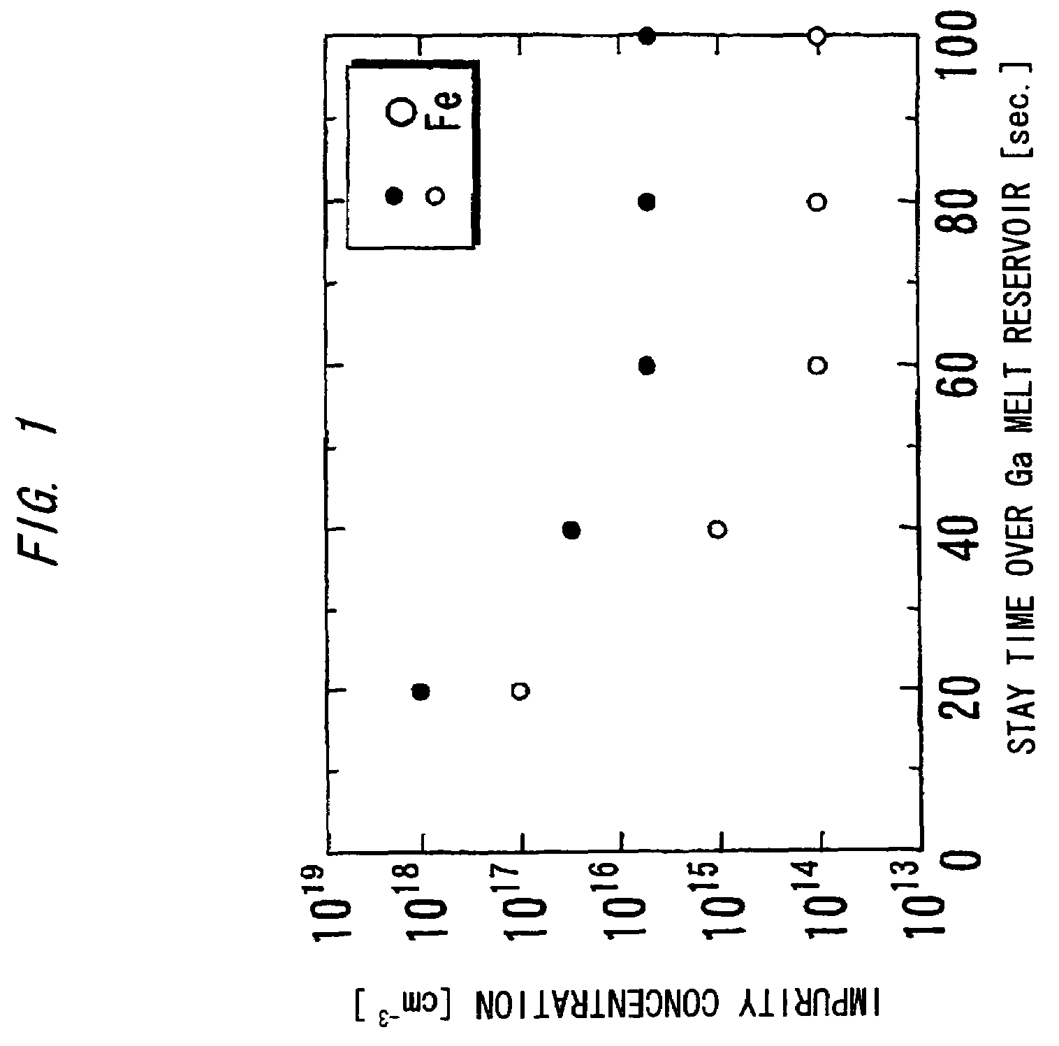
[0079]The HCl introducing tube 4 is halfway enlarged in its inside diameter to provide a Ga melt reservoir 6 to contain a Ga melt 7.

[0080]A substrate holder 9 with an underlying substrate 8 placed thereon is rotatably and movably disposed on the right side (i.e., downstream side) of the quartz reactor tube 1.

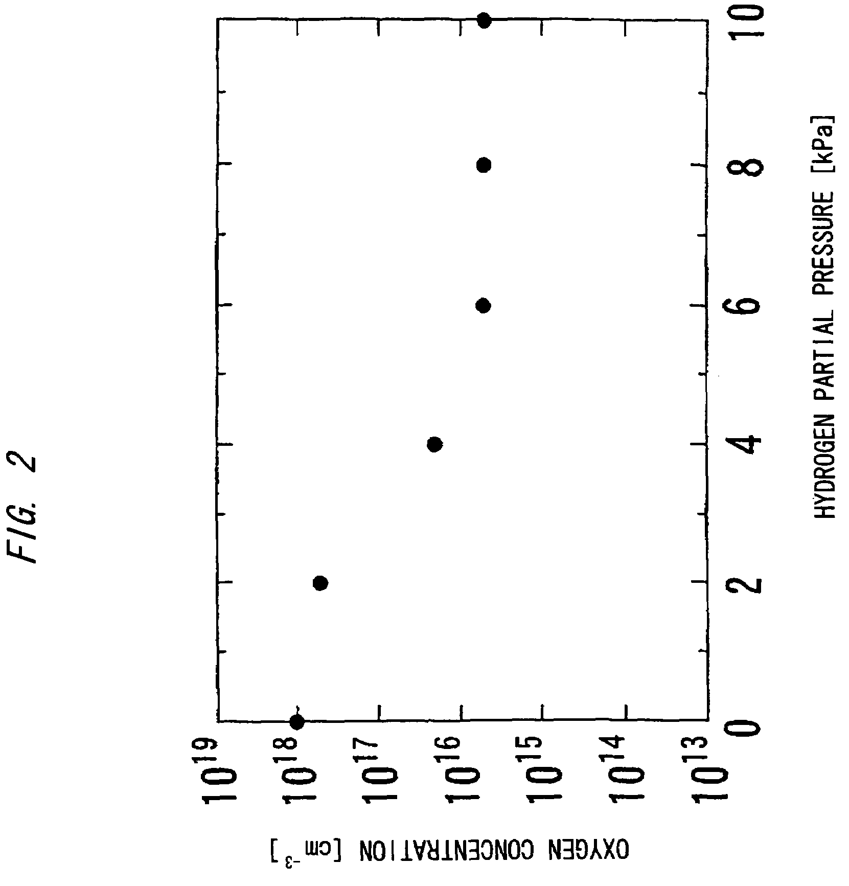
[0081]In growing GaN by using the HVPE reactor 10, the NH3 gas as the group V source is introduced through the NH3 int...

example 2

An Example to Use the Methods (a)+(b)+(c)

[0086]FIGS. 5A to 5G are cross sectional views showing a method of making a GaN self-standing substrate in Example 2 according to the invention.

[0087]A GaN self-standing substrate is made by a process as shown in FIGS. 5A to 5G.

[0088]First, a sapphire substrate 11 with a diameter of 2 inches is provided as an underlying substrate (FIG. 5A). Then, a GaN film 12 is formed 300 nm thick on the sapphire substrate 11 by MOVPE (FIG. 5B). Then, a Ti film 13 is vacuum-deposited 20 nm thick (FIG. 5C) thereon, and then heated at 1000 degree Celsius for 30 min. in a mixed atmosphere of H2 and NH3 (with H2 gas partial pressure of 80 kPa). By the heat treatment, the Ti film 13 on the surface of the substrate is nitrided such that it is changed into a porous TiN 14 with a number of microscopic pores with an inside diameter of tens of micrometers by the aggregation effect (FIG. 5D).

[0089]Then, it is placed in the HVPE reactor 10 as shown in FIG. 4 and a GaN ...


PUM

PropertyMeasurementUnit
diameteraaaaaaaaaa
thicknessaaaaaaaaaa
optical absorption coefficientaaaaaaaaaa

Abstract

A nitride-based semiconductor substrate having a diameter of 25 mm or more, a thickness of 250 micrometers or more, and an optical absorption coefficient of less than 7 cm−1 to light with a wavelength of 380 nm or more. The nitride-based semiconductor substrate is made by the HVPE method that uses gallium chloride obtained by reacting a Ga melt with a hydrogen chloride gas. The Ga melt is contacted with the hydrogen chloride gas for one minute or more to produce the gallium chloride.

Description

[0001]The present application is based on Japanese patent application No. 2005-319630 filed Nov. 2, 2005, the entire contents of which are incorporated herein by reference.BACKGROUND OF THE INVENTION[0002]1. Field of the Invention[0003]This invention relates to a nitride-based semiconductor substrate and, in particular, to a nitride-based semiconductor substrate that satisfies a high transparency and a high conductivity together. Also, this invention relates to a method of making the nitride-based semiconductor substrate.[0004]2. Description of the Related Art[0005]GaN-based compound semiconductors such as gallium nitride (GaN), indium gallium nitride (InGaN) and aluminum gallium nitride (AlGaN) attract attention for a material of blue light emitting diode (LED) or laser diode (LD). Further, since the GaN-based compound semiconductors have a good heat resistance and environment resistance, they have begun to be applied to other electronic devices.[0006]Thus far, the GaN-based compou...

Claims


Application Information

Patent Timeline
Patent Type & Authority Patents(United States)
IPC IPC(8): B32B9/00B32B19/00H01L33/32
CPCC30B25/02C30B29/406H01L21/0242H01L21/02491H01L21/02513H01L21/0254H01L21/0262H01L21/02639H01L21/02647
Inventor OSHIMA, YUICHI
Owner SUMITOMO CHEM CO LTD
Why Eureka
Try Eureka