Source/drain electrodes, transistor substrates and manufacture methods, thereof, and display devices

a transistor substrate and source electrode technology, applied in semiconductor devices, semiconductor device details, electrical apparatus, etc., can solve the problems of affecting the quality of displayed images, unable to establish an electrically ohmic contact if the aluminum oxide layer is exposed to oxidation, and high resistance to oxidation. , to achieve the effect of low resistance, high-performance display devices, and excellent productivity

Inactive Publication Date: 2010-03-23
KOBE STEEL LTD
View PDF31 Cites 38 Cited by
  • Summary
  • Abstract
  • Description
  • Claims
  • Application Information

AI Technical Summary

Benefits of technology

[0031]The present invention has been accomplished under these circumstances, and an object of the present invention is to provide an source / drain electrode that eliminates the need of the lower barrier metal layer, simplifies the manufacturing processes without increasing the number of steps, permits the direct and reliable connection between an aluminum alloy film and the amorphous silicon channel film, and ensures a low electrical resistivity even when the aluminum alloy film is subjected to a process at low temperatures of about 100° C. or higher and about 300° C. or lower. Specifically, the object is to provide a source / drain electrode that is suitable for processes at lower temperatures and reliably ensures a low electrical resistivity of the aluminum alloy film of 8 μΩ·cm or lower even when the aluminum alloy film is subjected to a heat treatment at low temperatures of, for example, about 200° C. for about twenty minutes.
[0032]Another object of the present invention is to provide a technique of eliminating the need of not only the lower barrier metal layer but also the upper barrier metal layer to thereby permit the direct and reliable connection of the aluminum alloy film not only to the amorphous silicon channel film but also to the transparent pixel electrode.
[0047]The source / drain electrodes according to the present invention have the above-mentioned configurations, thereby permit direct connection between the aluminum alloy thin film and the thin-film transistor semiconductor layer. In preferred embodiments, they further permit the direct connection between the aluminum alloy thin film and the transparent pixel electrode. They can therefore provide inexpensive, high-performance display devices with excellent productivity.
[0048]The source / drain electrodes according to the present invention further ensure a sufficiently low electrical resistivity even when heat treatment is carried out at relatively low temperatures of about 200° C. The term “heat treatment temperature” herein refers to the highest temperature during manufacturing processes of TFT array substrates. It corresponds to, for example, the temperature of heating the substrate in CVD film-deposition or the temperature of a heating furnace for thermosetting of the protecting film, in general manufacturing processes of thin-film transistor substrates for display devices.

Problems solved by technology

This is because, if an aluminum alloy thin film is directly connected to the transparent pixel electrode, the contact resistance between these components is high, which impairs the quality of displayed images.
Aluminum used as a material for the interconnections for the transparent pixel electrode is very susceptible to oxidation, and an insulating layer of an aluminum oxide is formed at the interface between the aluminum alloy thin film and the transparent pixel electrode.
The indium tin oxide (ITO) as a material for the transparent pixel electrode is an electrically conductive metal oxide, but it fails to establish an electrically Ohmic contact if the aluminum oxide layer is formed.
These extra units cause an increased production cost and a decreased productivity.
According to this technique, however, the ITO film that is most widely used must be replaced with the IZO film, which causes an increased material cost.
The method, however, requires an extra step for the surface treatment, which causes a decreased productivity.
This method, however, requires an extra step of depositing the second layer containing impurities.
To avoid this problem, the method requires frequent maintenance operations while stopping the film-deposition step, and this results in a significantly decreased productivity.
However, no technique has been disclosed that enables the direct contact between an amorphous silicon thin film and a source / drain interconnection containing an aluminum alloy.
The system including extra units for the deposition of barrier metal layers causes an increased production cost and a reduced productivity.
In addition, the tapering of the three-layered multilayer interconnection by wet etching requires different etchants (etching solutions) for the barrier metals and for the aluminum alloy, respectively, and further requires different etching baths suitable for the etchants, to thereby cause an increased cost.
However, this technique does not realize processing with high precision.
The above explanation has been made by taking a liquid crystal display device as a representative example, but the problems in the conventional techniques are in common in amorphous silicon thin-film transistor substrates used not only in liquid crystal display devices but also in other devices.

Method used


Image

  • Source/drain electrodes, transistor substrates and manufacture methods, thereof, and display devices
  • Source/drain electrodes, transistor substrates and manufacture methods, thereof, and display devices
  • Source/drain electrodes, transistor substrates and manufacture methods, thereof, and display devices

Examples


first embodiment

[0104]An embodiment of the amorphous silicon thin-film transistor substrates according to the present invention will be illustrated in detail with reference to FIG. 3.

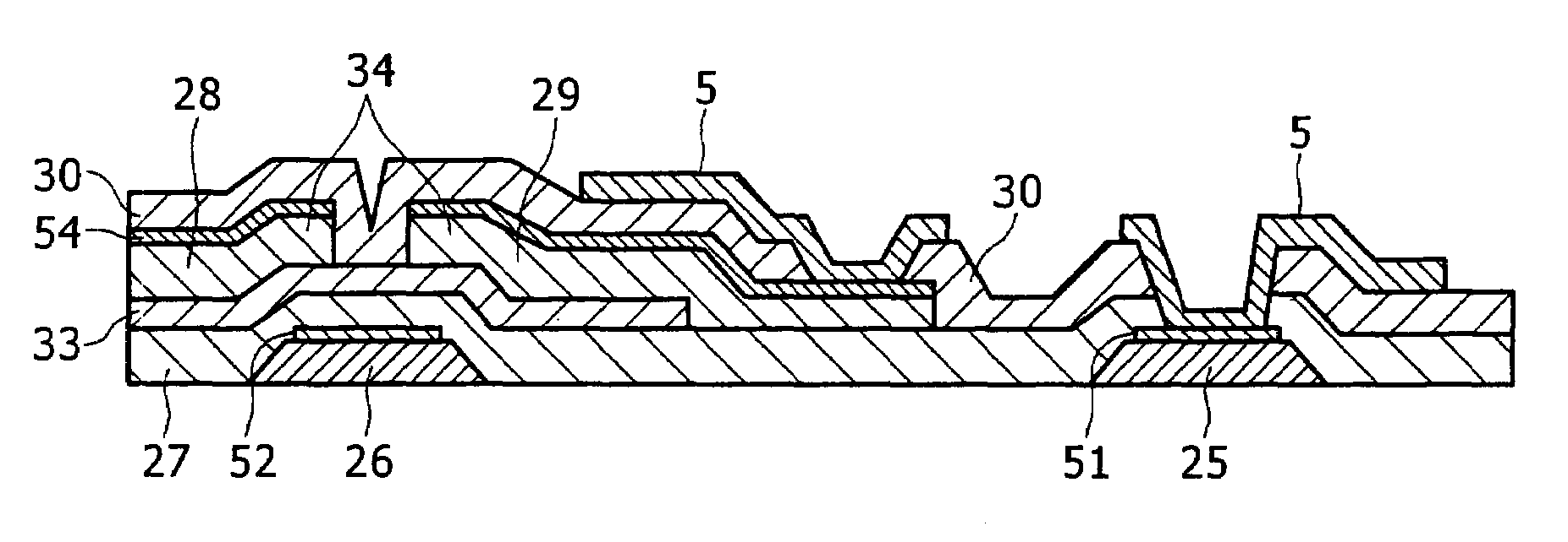
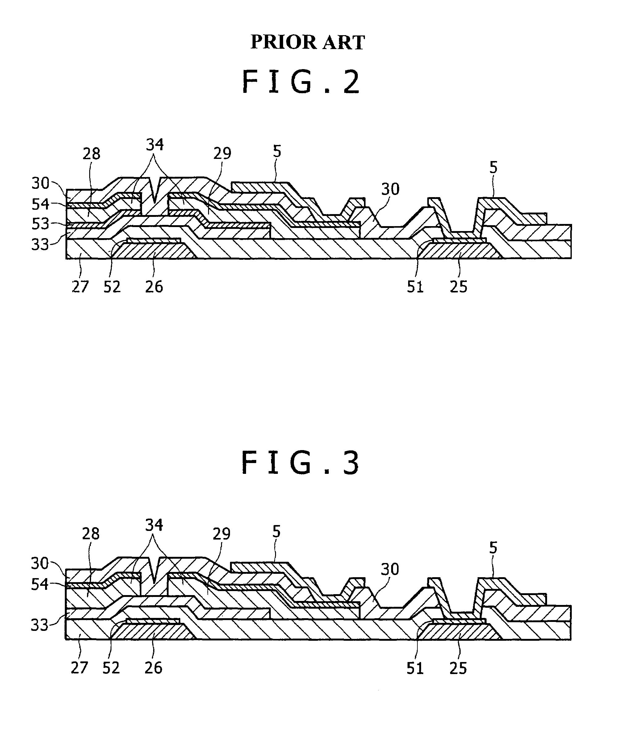
[0105]FIG. 3 is a schematic cross-sectional view illustrating a preferred embodiment of the thin-film transistor substrates according to the present invention. In FIG. 3, components corresponding to those in the conventional thin-film transistor substrate in FIG. 2 have the same reference numerals.

[0106]A comparison between FIG. 2 and FIG. 3 shows that the conventional thin-film transistor substrate comprises the lower barrier metal layer 53 made typically of molybdenum (Mo) below the source / drain electrodes (FIG. 2); whereas the thin-film transistor substrate according to the present invention does not include the lower barrier metal layer 53 (FIG. 3). This embodiment enables direct connection between the aluminum alloy and the channel amorphous silicon thin film without the interposition of the lower barrier metal la...

second embodiment

[0125]A thin-film transistor substrate according to Second Embodiment has the same configuration as the thin-film transistor substrate according to First Embodiment as illustrated in FIG. 2, except for not arranging both the upper barrier metal layer 54 and the lower barrier metal layer 53. The thin-film transistor substrate according to First Embodiment does not include the lower barrier metal layer 53 but includes the upper barrier metal layer 54.

[0126]The thin-film transistor substrate according to Second Embodiment can be prepared by the procedure of First Embodiment, except for forming an aluminum alloy thin film (Al-2.0 atomic percent Nd) having a thickness of about 300 nm alone on a glass substrate 1a and not forming a molybdenum film. In the thin-film transistor substrate according to Second Embodiment, the Al—Ni alloy thin film is directly connected not only to the amorphous silicon thin film but also to the transparent pixel electrode. This embodiment can not only eliminat...

experimental examples

Experimental Example 1

[0127]Experimental Example 1 and after-mentioned Experimental Example 2 were conducted so as to verify that excellent thin-film transistor properties, for example, can be obtained even without the lower barrier metal layer by using the thin-film transistor substrate according to First Embodiment. An Al-2.0 atomic percent Ni alloy was used as the source / drain electrode in Experimental Examples 1 and 2, and this alloy thin film is hereinafter briefly referred to as “Al—Ni alloy thin film”.

[0128]In Experimental Examples, the nickel content, the thicknesses of the nickel-enriched layer and aluminum oxide film were determined by RF glow discharge emission spectrometry (GD-OES) and observation on cross-sectional transition electron micrograph, respectively. The nickel content of the nickel-enriched layer and the oxygen content in the aluminum oxide film were determined by compositional analyses of cross-sectional transition electron micrographs by EDX.

[0129]Observati...


PUM

PropertyMeasurementUnit
electrical resistivityaaaaaaaaaa
temperaturesaaaaaaaaaa

Abstract

In a thin-film transistor substrate including a substrate, a thin-film transistor semiconductor layer, a source / drain electrode, and a transparent pixel electrode, the source / drain electrode includes a thin film of an aluminum alloy containing 0.1 to 6 atomic percent of nickel as an alloy element, and the aluminum alloy thin film is directly connected to the thin-film transistor semiconductor layer.

Description

BACKGROUND OF THE INVENTION[0001]1. Field of the Invention[0002]The present invention relates to source / drain electrodes and transistor substrates for use in thin-film transistors of liquid crystal displays, semiconductor devices, and optical components. It also relates to methods for manufacturing the substrates, and display devices using the substrates. Specifically, it relates to novel source / drain electrodes including an aluminum alloy thin film as a component.[0003]2. Description of the Related Art[0004]Liquid crystal display devices are used in a variety of applications ranging from small-sized mobile phones to large-sized television sets with 30-inch or larger screens. They are categorized by the pixel driving method into passive-matrix liquid crystal display devices and active-matrix liquid crystal display devices. Of these, active-matrix liquid crystal display devices having thin-film transistors (hereinafter briefly referred to as TFTs) as switching devices are widely used...

Claims


Application Information

Patent Timeline
Patent Type & Authority Patents(United States)
IPC IPC(8): H01L31/0224
CPCH01L23/53219H01L29/458H01L27/124H01L29/66765H01L29/4908H01L2924/0002H01L2924/00
Inventor KUGIMIYA, TOSHIHIROGOTOH, HIROSHI
Owner KOBE STEEL LTD
Why Eureka
Try Eureka