Low defect Si:C layer with retrograde carbon profile

a carbon profile, low defect technology, applied in the direction of basic electric elements, electrical apparatus, semiconductor devices, etc., can solve the problem of not severe retrograding, achieve enhanced electron mobility, increase electron mobility in the channel, and improve the effect of electron mobility

Active Publication Date: 2010-04-13
GLOBALFOUNDRIES U S INC
View PDF3 Cites 123 Cited by
  • Summary
  • Abstract
  • Description
  • Claims
  • Application Information

AI Technical Summary

Benefits of technology

[0009]To address the needs described above, the present invention provides an epitaxial Si:C layer with a high bulk carbon concentration from about 0.2% to about 5.0% in atomic concentration as well as a low defect density less than about 1.0×10⁹ / cm2 by retrograding the carbon concentration profile near the surface of the silicon substrate. Also, the present invention provides an embedded epitaxial Si:C layer with high bulk carbon concentration and low defect density within the source and drain regions of CMOS transistors. When such epitaxial Si:C layers are embedded into the source and drain of an NFET, the resulting uniaxial tensile stress in the channel of the NFET enhances the electron mobility, enabling a mobility enhanced NFET.
[0019]Conventional theory about the formation of defect generation during a solid phase epitaxy assumes defect nucleation at the growth front. The initial growth surface at the beginning of a solid phase epitaxy is the interface between the underlying crystal silicon and the amorphized material formed by the amorphization implant. Once the defects are nucleated, they extend toward the top surface with the growth surface as the growth surface moves during the solid phase epitaxy. An implication of this theory is that defects are clustered near the end-of-range of the preamorphization implant. Also, according to this theory, carbon implantation into an SOI substrate such that the end-of-range of the preamorphization implant falls within the buried oxide layer should eliminate most of the defects.

Problems solved by technology

While some retrograding of the carbon concentration can be observed in vertical profiles of the carbon concentration in the prior art, the degree of the retrograding is not severe but minor and occurs naturally as a result of the limitation of the tools used for ion implantation.

Method used


Image

  • Low defect Si:C layer with retrograde carbon profile
  • Low defect Si:C layer with retrograde carbon profile
  • Low defect Si:C layer with retrograde carbon profile

Examples


first embodiment

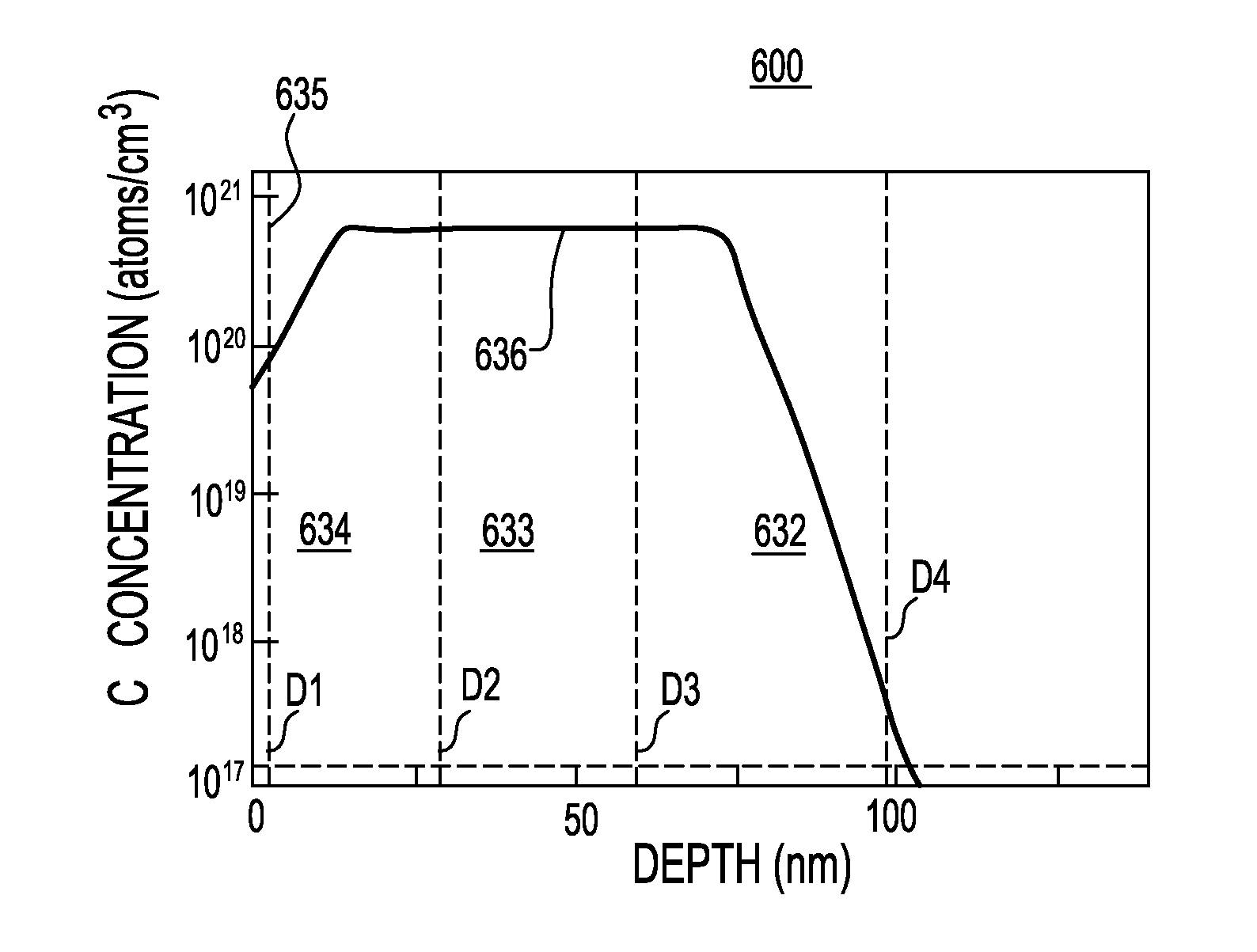
[0042]According to the present invention, a silicon substrate is provided in which carbon atoms are implanted by ion implantation. The silicon substrate may be a bulk substrate or a silicon-on-insulator substrate. FIG. 4 shows a bulk silicon substrate 400 with a carbon implanted silicon layer 436 and an underlying silicon layer 410 in which virtually no carbon is implanted. The boundary between the carbon implanted silicon layer 436 and the underlying silicon layer 410 is determined by the depth at which the carbon concentration is 3.5×10¹⁷ / cm3, or the solubility of carbon at the melting temperature of silicon. The thickness of the carbon implanted silicon layer 436 is the depth of the boundary between the carbon implanted silicon layer 436 and the underlying silicon layer 410.

[0043]In the case of a bulk silicon wafer, the carbon implanted silicon layer 436 is divided into four volumes of which the boundaries are represented by the four dotted lines in FIG. 4. The topmost dotted lin...

second embodiment

[0056]According to the present invention, a transistor structure 800 incorporating an active retrograde profile in the carbon concentration in Si:C layers is shown in FIG. 8. The transistor structure 800 comprises an underlying silicon layer 810, a buried oxide layer 820, a body of the transistor 830, a gate dielectric 842, a gate conductor stack 844, FET extensions 832, first spacers 852, second spacers 854, embedded Si:C layers without source / drain electrical doping 834, and embedded Si:C layer with source / drain electrical doping 836. Each of the two carbon substituted single crystal silicon layers includes both one of the embedded Si:C layers without source / drain electrical doping 834 and one of the embedded Si:C layers with source / drain electrical doping 836. While it is in principle possible to incorporate an Si:C layer only within the source or only within the drain, preferably both the source and drain incorporate an Si:C layer respectively.

[0057]Within the transistor structu...


PUM

PropertyMeasurementUnit
thicknessaaaaaaaaaa
thicknessaaaaaaaaaa
thicknessaaaaaaaaaa

Abstract

Formation of carbon-substituted single crystal silicon layer is prone to generation of large number of defects especially at high carbon concentration. The present invention provides structures and methods for providing low defect carbon-substituted single crystal silicon layer even for high concentration of carbon in the silicon. According to the present invention, the active retrograde profile in the carbon implantation reduces the defect density in the carbon-substituted single crystal silicon layer obtained after a solid phase epitaxy. This enables the formation of semiconductor structures with compressive stress and low defect density. When applied to semiconductor transistors, the present invention enables N-type field effect transistors with enhanced electron mobility through the tensile stress that is present into the channel.

Description

FIELD OF THE INVENTION[0001]The present invention relates to semiconductor structures and methods of manufacture, and more particularly to a carbon-substituted single crystal silicon layer (Si:C) and a metal-oxide-semiconductor field effect transistor (MOSFET) utilizing such carbon-substituted single crystal silicon layers (Si:C).BACKGROUND OF THE INVENTION[0002]Various techniques for enhancing semiconductor device performance through manipulation of carrier mobility have been investigated in the semiconductor industry. One of the key elements in this class of technology is the manipulation of stress in the channel of transistor devices. Some of these methods utilize a carbon-substituted single crystal silicon (Si:C) layer within a silicon substrate to change the lattice constant of the silicon material in the channel. While both silicon and carbon have identical electronic outer shells and the same crystal structure, that is, “the diamond structure,” their room temperature lattice ...

Claims


Application Information

Patent Timeline
Patent Type & Authority Patents(United States)
IPC IPC(8): H01L21/00
CPCH01L21/26506H01L29/1054H01L29/78696H01L29/7848H01L29/78618H01L29/78654H01L29/32H01L21/2022H01L21/02532H01L21/02529H01L21/02447H01L21/0245H01L21/02488H01L21/0251H01L21/02667H01L29/161H01L21/02675H01L21/02694
Inventor LIU, YAOCHENGIYER, SUBRAMANIAN S.LI, JINGHONG
Owner GLOBALFOUNDRIES U S INC
Why Eureka
Try Eureka