Flash memory system control scheme

a flash memory and control scheme technology, applied in the field of flash memory, can solve the problems of affecting the performance of the system, affecting and imposing physical performance limitations on the flash memory system b>10/b>, so as to improve the programming throughput of the flash memory system

Active Publication Date: 2010-09-21
MOSAID TECH
View PDF82 Cites 10 Cited by
  • Summary
  • Abstract
  • Description
  • Claims
  • Application Information

AI Technical Summary

Benefits of technology

[0019]It is an object of the present invention to obviate or mitigate at least one disadvantage of previous control schemes for Flash memory systems. In particular, it is an object of the present invention to improve Flash memory system programming throughput by interleaving programming operations in each Flash memory device of the system.
[0022]In a second aspect, the present invention provides a method for high speed wear leveling programming in a Flash memory system having a plurality Flash memory devices. The method includes receiving a data file having k pages, k being an integer greater than 0; selecting a programming profile corresponding to the size of k and configuration parameters of the Flash memory system; and programming at least one of the k pages of the data file in each of to at least two of the plurality of Flash memory devices in accordance with the selected programming profile.
[0026]In a fourth aspect, the present invention provides a method for high speed wear leveling programming in a Flash memory system having j Flash memory devices, where each of the j Flash memory devices has i pages per block, where j and i are integer values greater than 0. The method includes receiving a data file having k pages, k being an integer greater than 0; providing commands for programming k pages within z of j memory devices if a ceiling function of z=k / i is less than or equal to j; providing commands for programming j*i pages within j memory devices if the ceiling function of z=k / i is greater than j; updating k by setting k=k−(j*i); and repeating the step of programming updated k pages.

Problems solved by technology

Returning to the Flash memory system 10 of FIG. 1, there are specific issues that will adversely impact performance of the system.
The configuration of Flash memory system 10 imposes physical performance limitations.
With the large number of parallel signals running across the system, the signal integrity of the signals they carry will be degraded by crosstalk, signal skew, and simultaneous switching noise (SSN).
Power consumption in such a configuration becomes an issue as each signal track between the flash controller and flash memory devices is frequently charged and discharged for signaling.
With increasing system clock frequencies, the power consumption will increase as well.
From an architectural perspective, programming operations will take too much time.
There are two significant issues related to Flash programming.
First, Flash programming is slow relative to volatile memories such as DRAM and SRAM, and other non-volatile memories such as hard disk drives.
Therefore, programming large quantities of data to the Flash devices 16 may require a significant amount of time.
This linear file structure coupled with the relatively long programming time per page of the data file per memory device, results in a Flash memory system that requires significant time to store data.
Another issue which is related to the linear file structure is device reliability, and more specifically, program / erase wearing of one memory device relative to the other memory devices in the system.
Eventually, the memory cells will fail to function properly.
When memory device 52 fails, the entire system 50 is no longer usable since the memory devices are packaged together and replacement of a single memory device is impractical.
This is an unfortunate waste of memory devices, as the remaining devices in the system are still useful and may have significant life left.
This is referred to as block re-programming, which requires significant programming time and hence negatively impacts performance of the system.
Therefore, presently known Flash memory systems have slow throughput for programming data, and due to the unequal program and erase wearing across the devices, the entire system will have a lifespan limited to the first memory device to fail.

Method used


Image

  • Flash memory system control scheme
  • Flash memory system control scheme
  • Flash memory system control scheme

Examples


Embodiment Construction

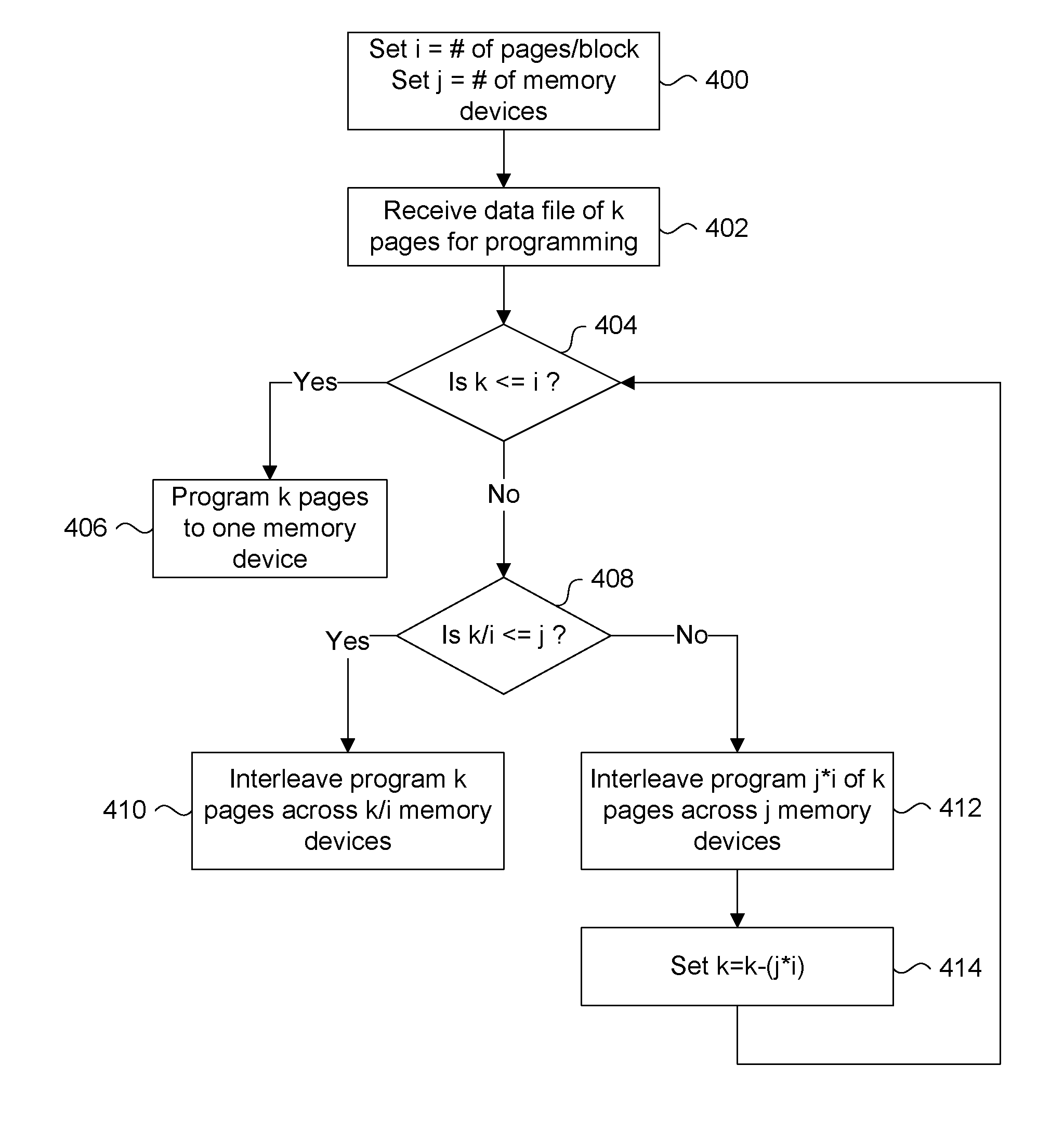
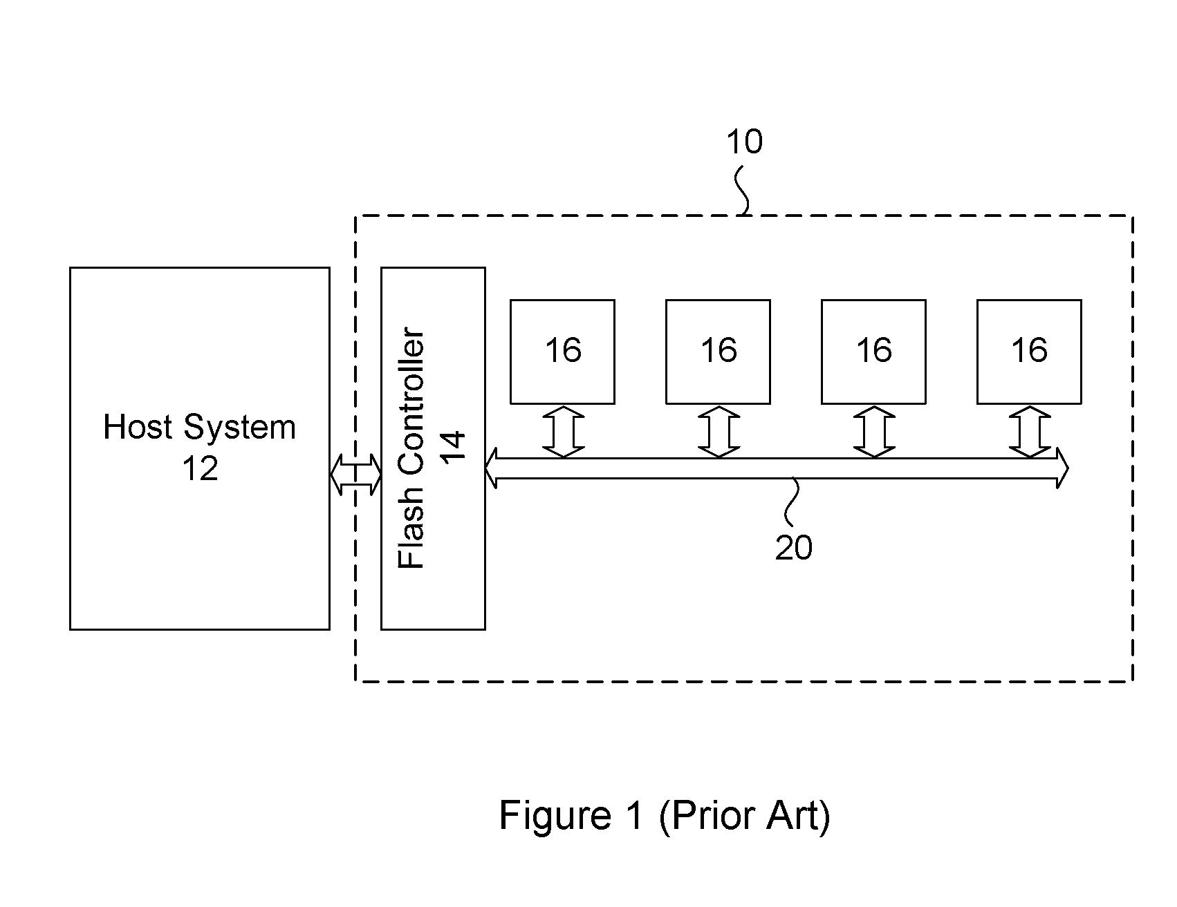
[0041]A Flash memory system architecture having serially connected Flash memory devices to achieve high speed programming of data. High speed programming of data is achieved by interleaving pages of the data amongst the memory devices in the system, such that different pages of data are stored in different memory devices. A memory controller issues program commands for each memory device in a bitstream having one or more signal lines. As each memory device receives a program command, it either begins a programming operation or passes the command to the next memory device. Therefore, the memory devices in the Flash system sequentially program pages of data one after the other, thereby minimizing delay in programming each page of data into the Flash memory system. The memory controller executes a wear level control algorithm to optimize programming performance and endurance for data of any size.

[0042]FIG. 4 is a block diagram of a Flash memory system having serially connected memory d...


PUM


Abstract

A Flash memory system architecture having serially connected Flash memory devices to achieve high speed programming of data. High speed programming of data is achieved by interleaving pages of the data to be programmed amongst the memory devices in the system, such that different pages of data are stored in different memory devices. A memory controller issues program commands for each memory device. As each memory device receives a program command, it either begins a programming operation or passes the command to the next memory device. Therefore, the memory devices in the Flash system sequentially program pages of data one after the other, thereby minimizing delay in programming each page of data into the Flash memory system. The memory controller can execute a wear leveling algorithm to maximize the endurance of each memory device, or to optimize programming performance and endurance for data of any size.

Description

CROSS REFERENCE TO RELATED APPLICATIONS[0001]This application claims the benefit of priority of U.S. Provisional Patent Application No. 60 / 788,083 filed Mar. 31, 2006, which is incorporated herein by reference in its entirety.FIELD OF THE INVENTION[0002]The present invention relates generally to Flash memory. More particularly, the present invention relates to a multi-device Flash memory system for mass storage applications.BACKGROUND OF THE INVENTION[0003]Flash memory is a commonly used type of non-volatile memory in widespread use as mass storage for consumer electronics, such as digital cameras and portable digital music players for example. The density of a presently available Flash memory chip can be up to 32 Gbits (4 GB), which is suitable for use in popular USB Flash drives since the size of one Flash chip is small.[0004]The advent of 8 mega pixel digital cameras and portable digital entertainment devices with music and video capabilities has spurred demand for ultra-high cap...

Claims


Application Information

Patent Timeline
Patent Type & Authority Patents(United States)
IPC IPC(8): G06F12/00G06F13/00G06F13/28
CPCG06F12/0246G11C7/1021G11C16/10G11C16/32G11C7/1042G06F2212/1036G06F2212/7211G11C2216/24G11C2216/22G11C16/04
Inventor KIM, JIN-KI
Owner MOSAID TECH
Why Eureka
Try Eureka