Thin-film transistor array, method of fabricating the same, and liquid crystal display device including the same

a technology of thin-film transistors and liquid crystal displays, which is applied in the direction of semiconductor devices, electrical equipment, instruments, etc., can solve the problems of unavoidable a number and increase of photolithography steps, and achieve the effect of enhancing reliability in electrical connections

Active Publication Date: 2010-09-28
NEC LCD TECH CORP
View PDF7 Cites 106 Cited by
  • Summary
  • Abstract
  • Description
  • Claims
  • Application Information

AI Technical Summary

Benefits of technology

[0015]In view of the above-mentioned problem in the related art, it is an exemplary object of the present invention to provide a thin-film transistor array which is capable of enhancing reliability in electrical connection with an external driver circuit, and being fabricated in accordance with a low-cost process without an increase in a number of carrying out a photolithography step.
[0022]The exposure to reducing plasma reduces an electrical conductivity of oxide semiconductor of which the source terminal, the gate terminal and the pixel electrode are composed, and accomplishes desired electric contact between the source and gate terminals and an external circuit terminal, that is, a small contact resistance between the same. Since oxide semiconductor of which the channel of a thin-film transistor is composed is not exposed to reducing plasma, the oxide semiconductor can keep a desired electrical conductivity required as a semiconductor. If the channel is exposed to reducing plasma, the channel would have a reduced electrical conductivity, resulting in that a drain off current of a thin-film transistor increases, and accordingly, it is not possible to keep a desired an ON / OFF ratio.
[0023]In a second exemplary aspect of the present invention, there is provided a method of fabricating a thin-film transistor array, including forming an oxide-semiconductor film, patterning the oxide-semiconductor film into a channel, a source and a drain of a thin-film transistor, a pixel electrode, a gate terminal, and a source terminal, and exposing at least a part of each of the source, the drain, the pixel electrode, the source terminal, and the gate terminal to one of reducing plasma and plasma containing at least one of B, Al, Ga, In and F for reducing a resistivity of the part.
[0024]There is further provided a method of fabricating a thin-film transistor array, including forming an oxide-semiconductor film, patterning the oxide-semiconductor film into a channel, a source and a drain of a thin-film transistor, a pixel electrode, a gate terminal, and a source terminal, and doping at least one of B, Al, Ga, In and F into at least a part of each of the source, the drain, the pixel electrode, the source terminal, and the gate terminal for reducing a resistivity of the part.

Problems solved by technology

However, the above-mentioned thin-film transistor array is accompanied with a problem that it is unavoidable for a number of carrying out a photolithography step to increase, since an electrically conductive part is formed by doping impurities thereinto through the use of a photomask.

Method used


Image

  • Thin-film transistor array, method of fabricating the same, and liquid crystal display device including the same
  • Thin-film transistor array, method of fabricating the same, and liquid crystal display device including the same
  • Thin-film transistor array, method of fabricating the same, and liquid crystal display device including the same

Examples


first exemplary embodiment

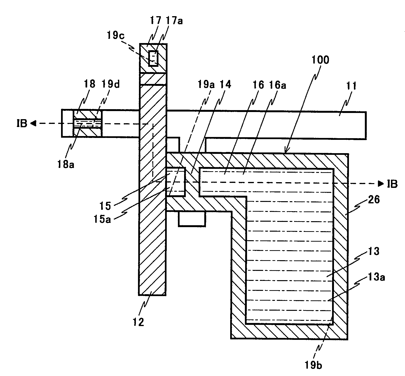
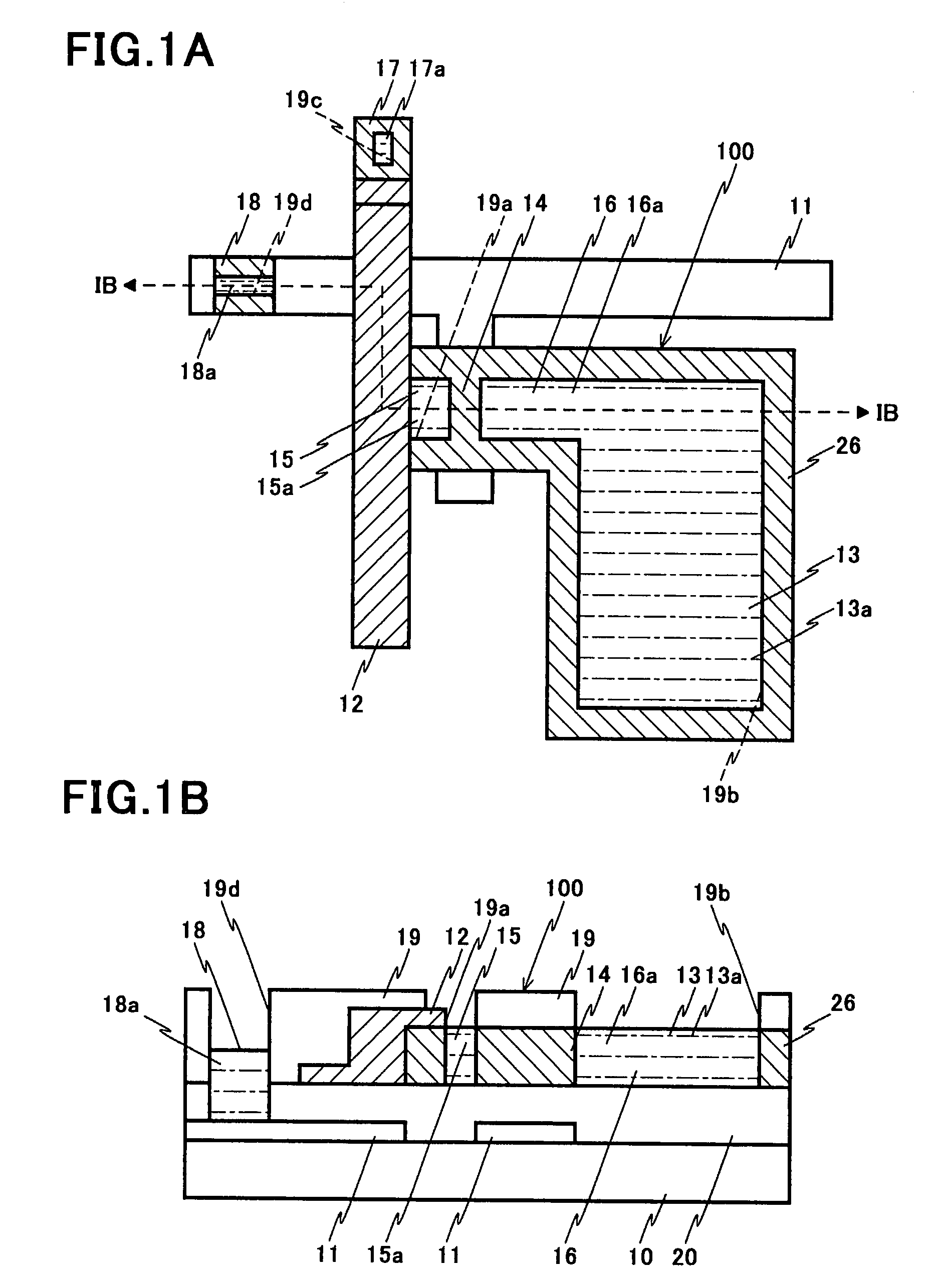
[0066]FIG. 1A is a plain view of a thin-film transistor array in accordance with the first exemplary embodiment, and FIG. 1B is a cross-sectional view taken along the line IB-IB in FIG. 1A.

[0067]The thin-film transistor array in accordance with the first exemplary embodiment is a bottom gate stagger type thin-film transistor array.

[0068]The thin-film transistor array in accordance with the first exemplary embodiment is designed to include a plurality of thin-film transistors 100 arranged in a matrix on an electrically insulating substrate 10, that is, the thin-film transistors 100 are arranged on the electrically insulating substrate 10 in both a column direction (for instance, an up-down direction in FIG. 1A) and a row direction which is perpendicular to the column direction in a plane in which the column direction lies (for instance, a left-right direction in FIG. 1A).

[0069]For simplification, FIGS. 1A and 1B illustrate only one thin-film transistor 100 and a structure existing ar...

second exemplary embodiment

[0121]Hereinbelow is explained a method of a thin-film transistor array in accordance with the second exemplary embodiment, with reference to FIGS. 6A to 9B.

[0122]The thin-film transistor array in accordance with the second exemplary embodiment is of a bottom gate planar type.

[0123]FIGS. 6A, 7A, 8A and 9A are plain views showing respective steps to be carried out in a method of fabricating the thin-film transistor array in accordance with the second exemplary embodiment, and FIGS. 6B, 7B, 8B and 9B are cross-sectional views taken along the lines VIB-VIB, VIIB-VIIB, VIIIB-VIIIB, and IXB-IXB, respectively.

[0124]Parts or elements in the second exemplary embodiment that correspond to those of the first exemplary embodiment have been provided with the same reference numerals.

[0125]First, as illustrated in FIGS. 6A and 6B, a gate metal film (defined as “an electrically conductive film” in claims) is formed on the electrically insulating substrate 10. For instance, the gate metal film is c...

third exemplary embodiment

[0144]Hereinbelow is explained a method of a thin-film transistor array in accordance with the third exemplary embodiment, with reference to FIGS. 10A to 13B.

[0145]The thin-film transistor array in accordance with the third exemplary embodiment is of a top gate planar type.

[0146]FIGS. 10A, 11A, 12A and 13A are plain views showing respective steps to be carried out in a method of fabricating the thin-film transistor array in accordance with the third exemplary embodiment, and FIGS. 10B, 11B, 12B and 13B are cross-sectional views taken along the lines XB-XB, XIB-XIB, XIIB-XIIB, and XIIIB-XIIIB, respectively.

[0147]Parts or elements in the third exemplary embodiment that correspond to those of the first exemplary embodiment have been provided with the same reference numerals.

[0148]First, as illustrated in FIGS. 10A and 10B, an amorphous ZnO film is formed by sputtering at room temperature on the electrically insulating substrate 10. The electrically insulating substrate 10 is comprised ...


PUM


Abstract

A thin-film transistor array includes an electrically insulating substrate, a plurality of thin-film transistors arranged in a matrix on the substrate, and each including a channel, a source, and a drain each comprised of an oxide-semiconductor film, a pixel electrode integrally formed with the drain, a source signal line through which a source signal is transmitted to a group of thin-film transistors, a gate signal line through which a gate signal is transmitted to a group of thin-film transistors, a source terminal formed at an end of the source signal line, and a gate terminal formed at an end of the gate signal line. The source terminal and the gate terminal are formed in the same layer as a layer in which the channel is formed. The source terminal and the gate terminal have the same electric conductivity as that of the pixel electrode.

Description

BACKGROUND OF THE INVENTION[0001]1. Field of the Invention[0002]The invention relates to a thin-film transistor array, a method of fabricating the same, and a liquid crystal display device including the same.[0003]2. Description of the Related Art[0004]A transparent electrically conductive film composed of oxide, such as an ITO film composed of compound of indium (In), tin (Sn), and oxygen (O), is frequently used in a flat panel display or a photoelectric transfer device, since it has a sheet resistance of a few ohms per a unit area even if it has a small thickness such as hundreds of nanometers, and it has high transmittance to visible light.[0005]Furthermore, a study to a thin-film transistor including a channel layer composed of transparent oxide semiconductor such as In—Ga—Zn—O has been recently started.[0006]Such oxide semiconductor contains highly ionic bonds, and is characterized by a small difference in electron mobility between crystalline state and amorphous state.[0007]Ac...

Claims


Application Information

Patent Timeline
Patent Type & Authority Patents(United States)
IPC IPC(8): H01L31/00
CPCH01L29/78618H01L27/124H01L27/1288H01L27/1225H01L29/7869
Inventor TAKECHI, KAZUSHIGENAKATA, MITSURU
Owner NEC LCD TECH CORP
Why Eureka
Try Eureka