

Method for forming fine copper particle sintered product type of electric conductor having fine shape, and process for forming copper fine wiring and thin copper film by applying said method
a technology of electric conductor and product type, applied in the direction of superimposed coating process, resistive material coating, liquid/solution decomposition chemical coating, etc., can solve the problems of not finding a way to completely prevent surface oxidation, not yet reaching practical levels, and easy oxidation of copper, etc., to achieve high yield, high reproducibility, and sufficient reaction rate
- Summary
- Abstract
- Description
- Claims
- Application Information
AI Technical Summary
Benefits of technology
Problems solved by technology
Method used
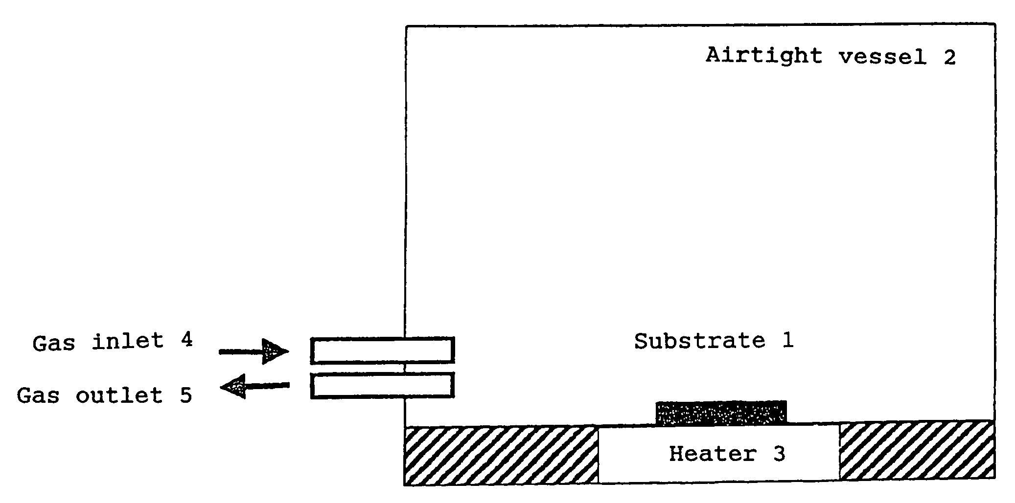
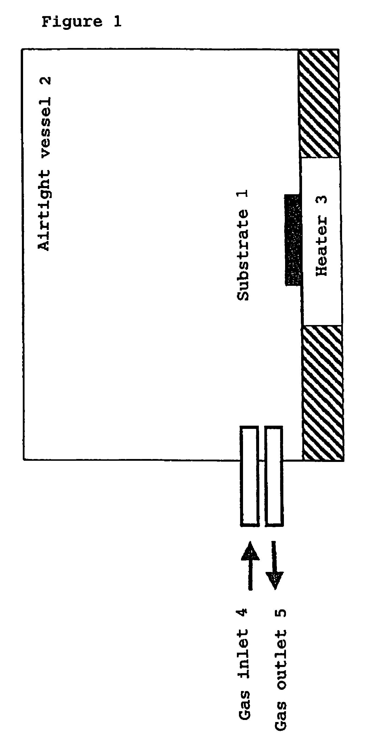
Image

Examples
examples 1-1 to 1-4
and Comparative Examples 1-1 to 1-3
Reduction / Baking Treatment in Vapor of Organic Compound
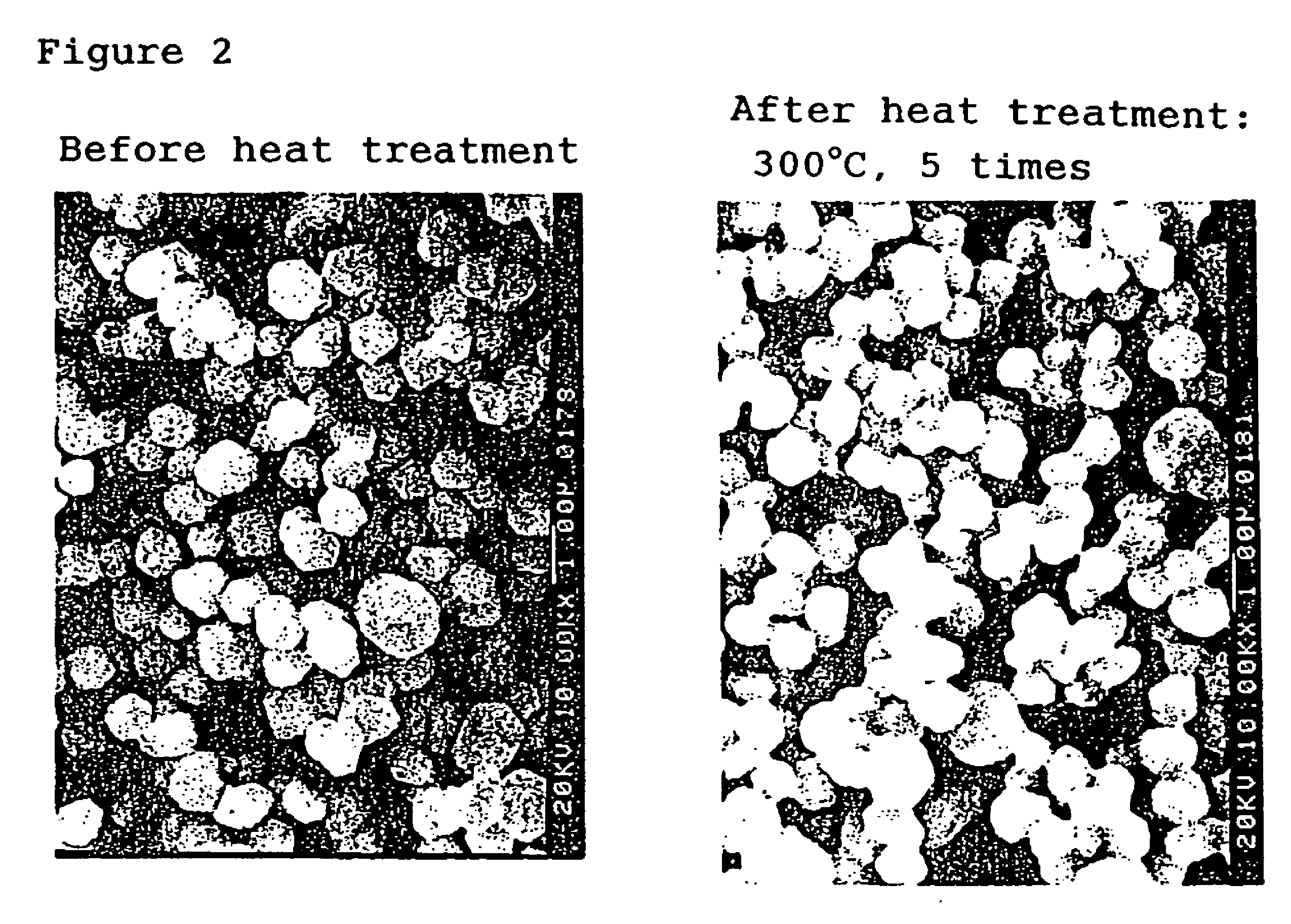
[0117]A commercially available dispersion of copper ultra fine particles (brand name: independently dispersed ultra fine particle, Perfect copper made by Ulvac Materials, Inc.) was used, which is specifically a dispersion of copper nano-particles having a surface oxide film layer with an average particle diameter of 5 nm, containing 100 parts by mass of copper fine particles partially having an oxide film layer on the surface, 15 parts by mass of dodecylamine (the molecular weight of 185.36 and the boiling point of 248° C.) as an alkyl amine, and 75 parts by mass of mineral spirit as an organic solvent.
[0118]To 100 parts by mass of a dispersion of the copper ultra fine particles, 5 parts by mass of toluene was added, and then 100 parts by mass of methanol was added to precipitate the contained copper fine particles. With respect to 80 parts by mass of the copper fine particles, which is collect...
examples 1-5 to 1-11
and Comparative Example 1-4
Reduction / Baking in Presence of Organic Compound Contained in Coated Layer
[0124]At first, an aqueous dispersion containing copper ultra fine particles was prepared by a wet reductive reaction. After 30 g of copper sulfate was dissolving in 100 ml of distilled water, 100 g of diethanolamine was added as a reducing agent into the aqueous solution which was heated to 80° C. Subsequently, a wet reductive reaction was proceeded for eight hours while stirring was continued, and a dark brown aqueous dispersion containing formed copper fine particles was obtained. Acetone was added into the dispersion to remove diethanolamine and precipitate copper fine particles. The cleaning operation with the use of acetone was repeated three times to remove a remaining raw material, a by-product due to a reaction and impurities. The obtained copper fine particles had a surface oxide film layer partially on the surface, which is oxidized copper, and had the average particle dia...
example 1-12
Reduction / Baking Treatment in Vapor of Organic Compound
[0131]A commercially available dispersion of copper ultra fine particles (brand name: independently dispersed ultra fine particle Perfectcopper, made by Ulvac Materials, Inc.) was used, which is a dispersion of copper nano-particles having partially an oxide film layer with an average particle diameter of 5 nm on the surface, specifically containing 100 parts by mass of copper fine particles, 15 parts by mass of dodecylamine (the molecular weight of 185.36 and the boiling point of 248° C.) for an alkyl amine, and 75 parts by mass of mineral spirit as an organic solvent.
[0132]To 100 parts by mass of a dispersion of the copper ultra fine particles, 5 parts by mass of toluene was added, and then 100 parts by mass of methanol was added to precipitate the contained copper fine particles. With respect to 80 parts by mass of the copper fine particles, which was collected by removing a supernatant liquid, and removing a remaining solven...
PUM
| Property | Measurement | Unit |
|---|---|---|
| particle diameter | aaaaa | aaaaa |
| temperature | aaaaa | aaaaa |
| width | aaaaa | aaaaa |
Abstract
Description
Claims
Application Information