Method for forming an iridium oxide (IrOx) nanowire neural sensor array

a neural sensor and nanowire technology, applied in the field of integrated circuit (ic) fabrication, can solve the problems of easy damage to the retina, limited surface area of the maximum charge an electrode can deliver, and tissue resistance to electrical stimulation is very high, so as to improve the surface to volume ratio, improve the resolution, and stimulate the effect of targeted areas

Inactive Publication Date: 2011-03-15
SHARP KK
View PDF11 Cites 15 Cited by
  • Summary
  • Abstract
  • Description
  • Claims
  • Application Information

AI Technical Summary

Problems solved by technology

One major difficulty with the epiretinal approach is that the tissue has a very high resistance to electrical stimulation.
The power output needs to be strictly controlled, since heat dissipation is limited in the subretinal space, and overheating can easily damage the retina.
One technical challenge is the trade-off between electrode density and stimulation charge.
Although the total charge injection required to elicit a visual percept is fixed, the maximum charge an electrode can deliver is limited by its surface area.
Surpassing this charge density threshold generates undesirable and irreversible electrochemical reactions.
Compared to IrOx, the performance of Pt is limited because it cannot sustain as much reversible faradic charge, and it catalyzes water electrolysis at low voltages, limiting its charge-injection capability.
However, because it relies heavily on faradic reactions, IrOx is slower in delivering current.
However, a key issue to be resolved is the fabrication of an electrode array that can conform to the concave shape of the foveal pit.
Another limitation associated with micromachining technology is size, as the individually machined electrodes cannot be made to a nano-size resolution.
Even if a template of nano-sized structures could be micro-machined, plating an array of nanostructures, with a noble metal for example, in a sufficiently high aspect ratio is a big challenge.
Some challenges facing conventional neuron stimulating and recording electrodes are the lack of resolution in micro-fabricated structures.
Poor resolution makes in impossible to stimulate subcellular regions of a single cell.
However, CNTs are prone to bending and warping, and lack the robustness required for repeatable sensitive electrical measurements.
However, it is difficult to form single-crystal IrO2 films using conventional PVD or electrode plating methods.
IrO2 nanostructures can be formed using a solution method, but these structures have a low mechanical strength and poor crystal quality.
Vapor phase transport methods can also be used to form IrO2 nanostructures, but this process requires high substrate temperature, and it is not suitable for use with glass and polyimide substrates.

Method used


Image

  • Method for forming an iridium oxide (IrOx) nanowire neural sensor array
  • Method for forming an iridium oxide (IrOx) nanowire neural sensor array
  • Method for forming an iridium oxide (IrOx) nanowire neural sensor array

Examples


Embodiment Construction

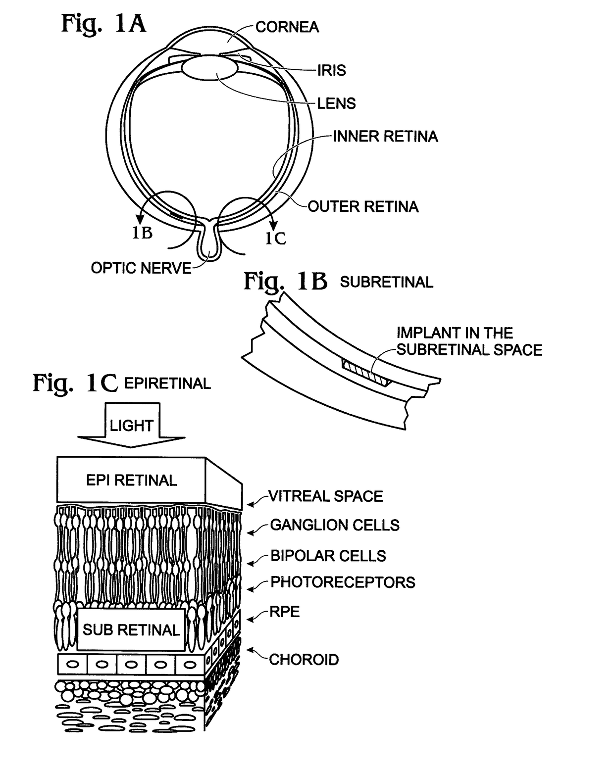
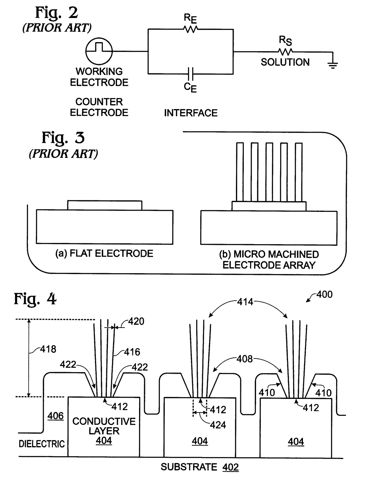
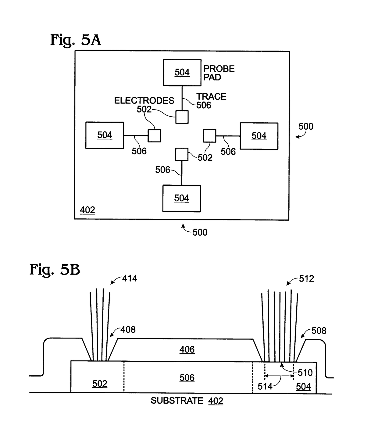
[0031]FIG. 4 is a partial cross-sectional view of an iridium oxide (IrOx) nanowire neural sensor array. The array 400 comprises a substrate 402 and a conductive layer 404 overlying the substrate 402. A dielectric layer 406 overlies the conductive layer 404. Contact holes 408 with sloped walls 410 are formed in the dielectric layer 406, exposing regions 412 of the conductive layer 404. IrOx nanowire neural interfaces 414 are shown, grown from the exposed regions 412 of the conductive layer 404. With respect to IrOx, typically x is ≦4. Although only 3 interfaces 414 are shown, the array is not limited to any particular number of interfaces. A nanowire may alternately be known as a nanostructure, nanorod, nanotip, or nanotube.

[0032]The average IrOx nanowire 416 has an aspect ratio in a range of about 1:1 to about 1:1000. As used herein, aspect ratio is defined as the ratio of the nanowire height 418, to the nanowire diameter or width 420 at proximal end 422 (base) attached to the condu...


PUM

PropertyMeasurementUnit
areaaaaaaaaaaa
diameteraaaaaaaaaa
chargeaaaaaaaaaa

Abstract

An iridium oxide (IrOx) nanowire neural sensor array and associated fabrication method are provided. The method provides a substrate with a conductive layer overlying the substrate, and a dielectric layer overlying the conductive layer. The substrate can be a material such as Si, SiO2, quartz, glass, or polyimide, and the conductive layer is a material such as ITO, SnO2, ZnO, TiO2, doped ITO, doped SnO2, doped ZnO, doped TiO2, TiN, TaN, Au, Pt, or Ir. The dielectric layer is selectively wet etched, forming contact holes with sloped walls in the dielectric layer and exposing regions of the conductive layer. IrOx nanowire neural interfaces are grown from the exposed regions of the conductive layer. The IrOx nanowire neural interfaces each have a cross-section in a range of 0.5 to 10 micrometers, and may be shaped as a circle, rectangle, or oval.

Description

BACKGROUND OF THE INVENTION[0001]1. Field of the Invention[0002]This invention generally relates to integrated circuit (IC) fabrication and, more particularly, to a fine resolution sensor with an iridium oxide nanowire neural interface.[0003]2. Description of the Related Art[0004]FIGS. 1A through 1C depict the placement of optical electrodes, using epiretinal and subretinal approaches (prior art). Studies show that blind patients with retinitis pigmentosa and masular degeneration can observe a visual percept induced by the direct electrical stimulation of the retina. Recently, retinal prosthesis development has progressed along two directions. The epiretinal approach places electrode in the vitreous fluid, attached to the surface of the retina, while the subretinal approach places electrodes on the outside of retina, wedged between the photoreceptors and the pigment epithelium. FIG. 1C shows the electrode positions for both type of retina prosthesis.[0005]One major difficulty with t...

Claims


Application Information

Patent Timeline
Patent Type & Authority Patents(United States)
IPC IPC(8): H01K3/10
CPCA61N1/0543B82Y15/00B82Y30/00Y10T29/49167Y10T29/49169Y10T29/49128Y10T29/4913Y10T29/49165G01N33/48728Y10T428/24998
Inventor ZHANG, FENGYANULRICH, BRUCE D.GAO, WEIHSU, SHENG TENG
Owner SHARP KK
Why Eureka
Try Eureka