Light emitting film, luminescent device, method for manufacturing light emitting film and method for manufacturing luminescent device

a technology of light-emitting film and luminescent device, which is applied in the direction of discharge tube luminescnet screen, discharge tube/lamp details, luminescent composition, etc., can solve the problems of deterioration of resin, more time and energy, and deterioration of film color and deterioration, so as to improve light-outgoing efficiency and reduce the effect of deterioration

Inactive Publication Date: 2011-04-12
NICHIA CORP
View PDF26 Cites 23 Cited by
  • Summary
  • Abstract
  • Description
  • Claims
  • Application Information

AI Technical Summary

Benefits of technology

[0015]The luminescent film consists principally of an inorganic substance, and metallic element composing the hydroxide oxide has a constant ionic charge number. Accordingly, since the luminescent film is stable due to suppression of oxidation-reduction reaction of compound after formation of the film, it is possible to provide a luminescent film which does not deteriorate even in the case of light with high density or driving at high temperature.
[0086]Impregnation can be performed in a vacuum in the third step. This can provide easy impregnation of voids of the inorganic binder layer with the resin. Although this reason is not clear, it is considered that a capillary phenomenon provides this effect. The “gel” refers to a colloidal system consisting of a solid and a liquid in more solid form than a sol.

Problems solved by technology

However, since conventional white light emitting apparatuses employ resin much, there is a problem that the resin deteriorates in the case where a light emitting element with high power or light with short wavelength.
In the case where a cured film which employs an inorganic group binder, in particular silica gel (SiO2), is used, there is a problem that the film is colored and deteriorates, and then darkens in exposure to high power or ultraviolet rays.
This requires more time and energy.
In addition, there is a problem that high temperature affects the semiconductor light emitting element or phosphor.
For example, lead wires bonded to the LED chip can be damaged by the heat, or the phosphor deteriorates.
Accordingly, in terms of reaction temperature, it is difficult to vitrify the sol to obtain inorganic polycrystalline by proceeding of the sol-gel reaction for improvement of light-outgoing efficiency.
Even if it is vitrified to obtain inorganic polycrystalline by proceeding of the sol-gel reaction, various problems arise in the interface between the luminescent film and the light emitting element.
The problems arise, for example, total reflection occurs in the vitrified interface, thus, the light-outgoing efficiency and the extraction of reduces, or a space layer is formed in the interface of the light emitting element or the phosphor by a cause of the cure, thus, the space layer obstructs outgoing of the light.
Additionally, in the construction where the light emitting element such as LED excites a luminescent layer, there is also a problem that the luminescent layer deteriorates in exposure to high energy of excitation light from the LED.
Since the light emitting layer that deteriorates becomes colored and turns to blackish, its original transparent characteristics deteriorates, thus, the light-outgoing efficiency reduces.
Even if typical resins are used as a molding member which molds the phosphor in the light emitting layer, the resins remarkably deteriorate in exposure to high-power light.
Accordingly, it is difficult to use resins as the molding member.
However, when exposed to high-power light from LED for a long time, a silica binder layer is colored and deteriorates.
As mentioned above, since Si is prone to be oxidized and reduced, that reason is considered that oxygen omission which occurs in the silica gel causes color deterioration.
When color deterioration occurs, the problem that the light output from the light emitting element reduces arises.
Further, recently, a light emitting apparatus which uses a high-power light emitting element has been developed, it tends to accelerate the deterioration of resin by the light from the light emitting element.
If typical resins are employed, the resins remarkably deteriorate in exposure to high-power light.
Accordingly, it is difficult to use these resins as the coating film.

Method used


Image

  • Light emitting film, luminescent device, method for manufacturing light emitting film and method for manufacturing luminescent device
  • Light emitting film, luminescent device, method for manufacturing light emitting film and method for manufacturing luminescent device
  • Light emitting film, luminescent device, method for manufacturing light emitting film and method for manufacturing luminescent device

Examples


first embodiment

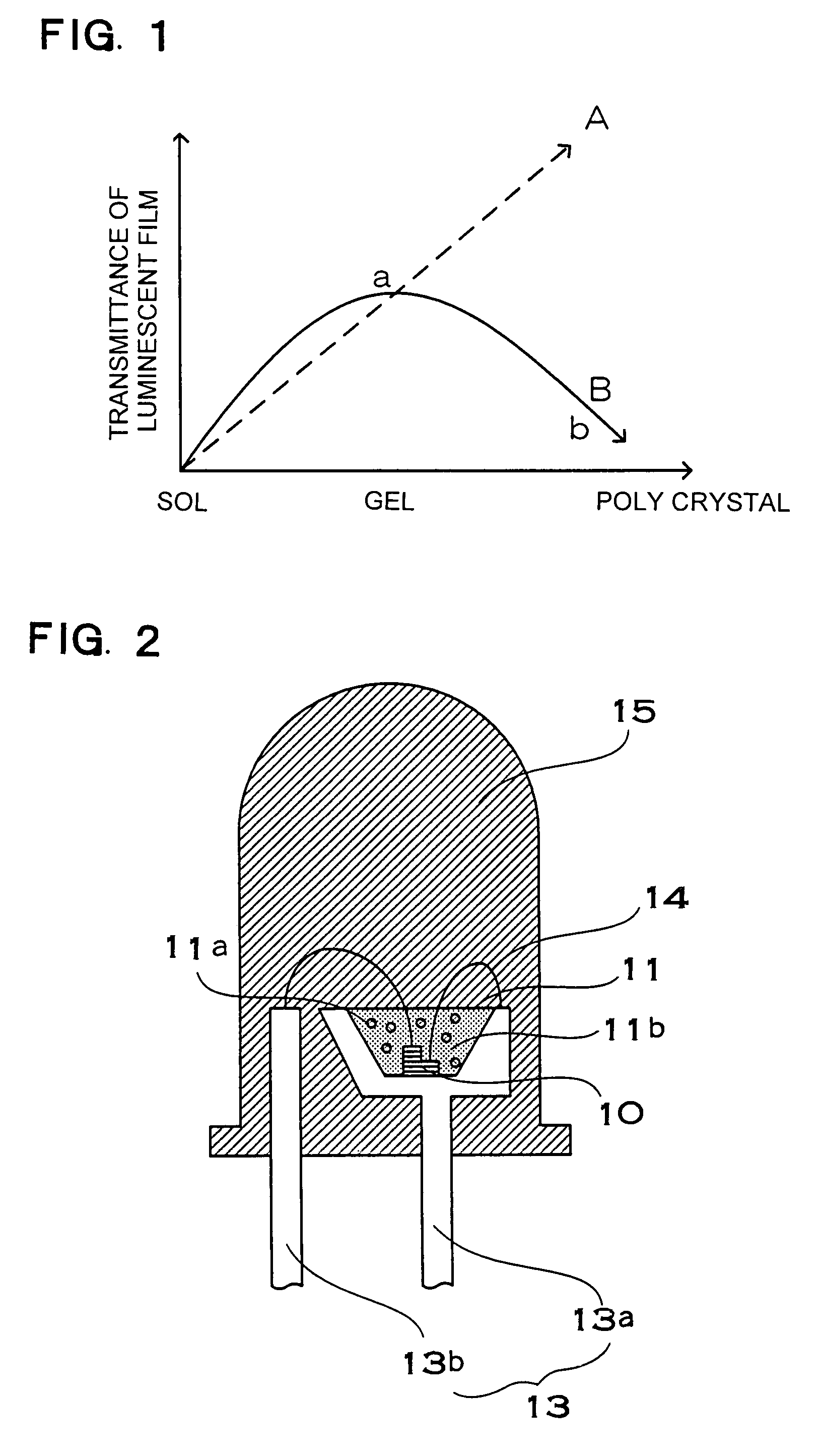
[0154]With reference to FIG. 2, a light emitting apparatus according to a first embodiment of the present invention is now described. The light emitting apparatus of first embodiment includes a light emitting element 10, the phosphor 11a, and the phosphor member 11 composed of the transparent binder 11b containing the phosphor 11a.

[0155]The light emitting element 10 composed of a bullet-shaped LED, for example, is mounted in a substantially central part of a cup disposed on the upper part of a mount lead 13a by die-bonding. The electrodes formed in the light emitting element 10 are electrically connected to the mount lead 13a and an inner lead 13b of a lead frame 13 with conductive wires 14. The Phosphor 11a contains a YAG group phosphor and a nitride group phosphor which absorb at least a part of light emitted light in the light emitting element 10 and emit luminescent radiation of wavelength different from the absorbed light. In addition, the nitride group phosphor can be coated ...

second embodiment

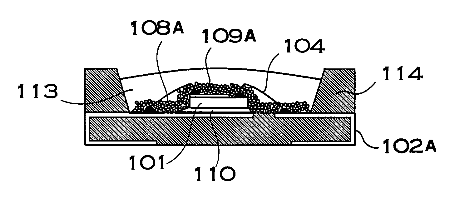
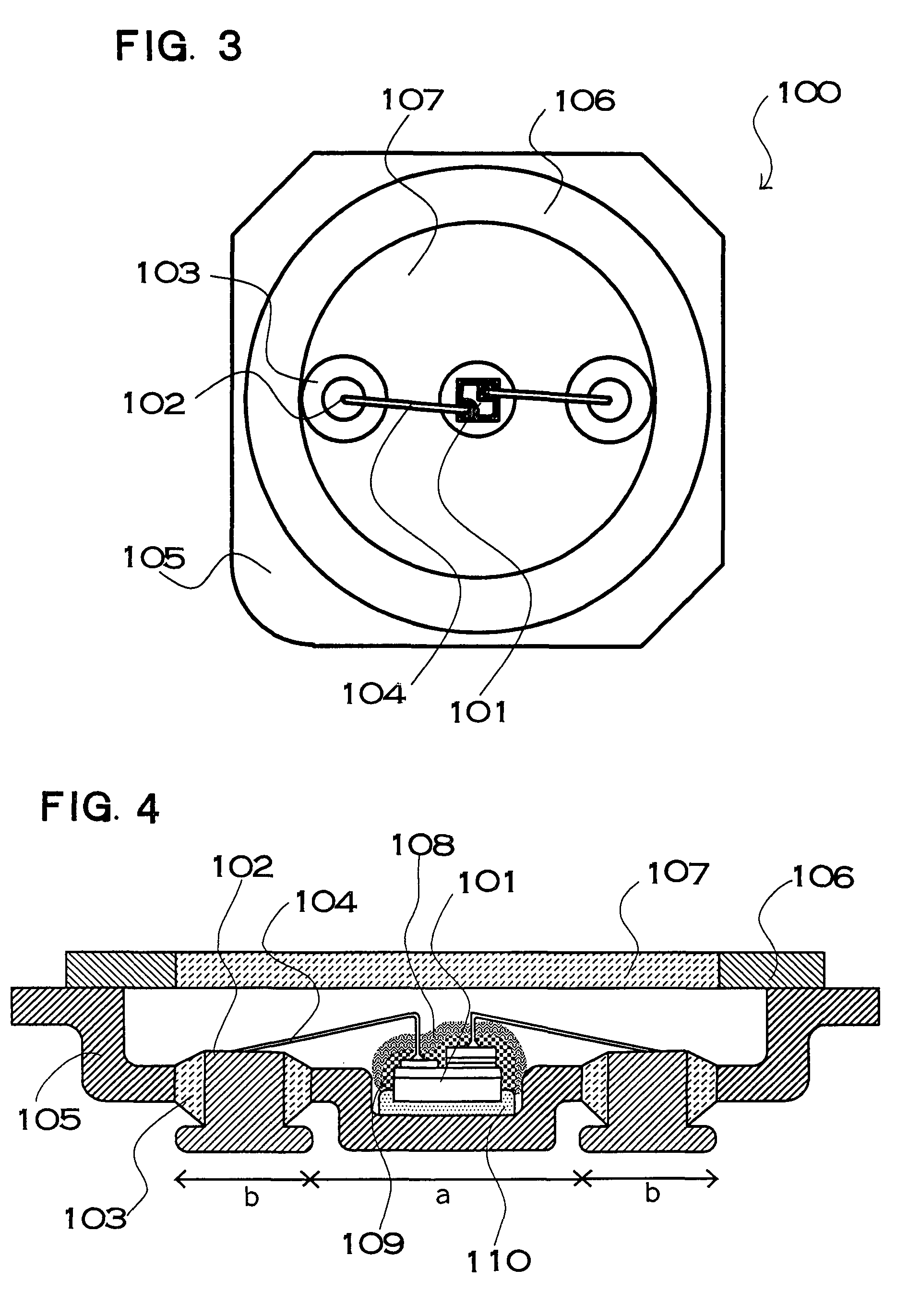
[0227]FIGS. 3 and 4 show a schematic plan view and a schematic cross-sectional view showing the structure in the state where an LED as light emitting element is mounted in a metal package, as an example of light emitting apparatus according to a second embodiment of the present invention.

[0228]A package 105 is formed of metal and has a recessed portion a in the center. A base portion b is located around said recessed portion. The base portion b has the two through holes penetrating in the thickness direction. The through holes are opposed to each other so as to sandwich said recessed portion a. The positive and negative lead terminals 102 are inserted into the through holes, respectively, so as to interpose hard glass, which is an insulating member 103, between each lead terminal and the through hole. A lid 106 composed of a transparent window portion 107 and a metal portion is located in the principal plane side of the metal package 105. The light emitting element, or the like, in ...

third embodiment

[0275]With reference to FIGS. 8 and 9, a light emitting apparatus according to a third embodiment of the present invention is described. FIG. 8 is a plan view of the light-emitting apparatus. FIG. 9 is a cross-sectional view of the light emitting apparatus of FIG. 8 as seen along the line A-A′. A phosphor member used in the light emitting apparatus according to the third embodiment can be used the phosphor member same as in the first embodiment. A light emitting element 401, which has an InGaN group semiconductor layer with light emission peak of 460 nm in the blue range as a light emitting layer, is used. A p-type semiconductor layer and an n-type semiconductor layer (not shown) are formed in the light emitting element 401. The conductive wires 404 connected to lead terminals 402 are formed on the p-type semiconductor layer and the n-type semiconductor layer. An insulating mold material 402 is formed so as to cover the peripheral of the lead terminal 403, and prevents a short circu...


PUM

PropertyMeasurementUnit
weight ratioaaaaaaaaaa
temperatureaaaaaaaaaa
light-emission wavelengthaaaaaaaaaa

Abstract

The present invention provides a reliable, long-life phosphor, or the like, which is prevented from darkening due to aging. A light emitting apparatus has a light emitting element and a phosphor layer. The phosphor layer has a phosphor excited by light from the light emitting element, and a binder which binds the phosphor. The binder is hydroxide oxide gel obtained by curing sol of a hydroxide oxide mixed with sol containing at least one metallic element selected from the group consisting of Al, Y, Gd, Lu, Sc, Ga, In, and B. Transmittance of hydroxide oxide in a gel state is higher than the transmittance in the polycrystal state where the sol-gel reaction is proceeded. In addition, the content of hydroxyl group or water of crystallization in the hydroxide oxide is 10% or less by weight.

Description

TECHNICAL FIELD[0001]The present invention relates to a luminescent film and a light emitting apparatus, which can be applied to a light source for lighting, an LED display, a back light source, a signal light, an illuminated switch, various sensors, various indicators, and so on, and a method for production of the luminescent film and light emitting apparatus.BACKGROUND ART[0002]A light emitting apparatus which radiates light with color different from the light of a light emitting element has been developed. The light emitting apparatus converts a part of the light of the light emitting element into a different wavelength by a phosphor, and mixes the light with converted wavelength and the light with non-converted wavelength of the light emitting element (for example, Japanese Laid-Open Publication Kokai No. 2002-198573). For example, a while LED light emitting apparatus, which has a blue light emitting diode (hereinafter, occasionally referred to as an “LED”) and a phosphor member...

Claims


Application Information

Patent Timeline
Patent Type & Authority Patents(United States)
IPC IPC(8): H01J1/62C09K11/02C09K11/08C09K11/77H01L33/50
CPCC09K11/02C09K11/0811C09K11/0844C09K11/0855C09K11/7728H01L33/501H01L2224/8592H01L2224/48091H01L2224/48247H01L2224/49107H01L2924/00014H01L2924/181H01L2224/48257H01L2924/00012
Inventor TAMAKI, HIROTOSOFUE, SHINSUKEIZUNO, KUNIHIROTAKEICHI, JUNJI
Owner NICHIA CORP
Why Eureka
Try Eureka