Schottky barrier quantum well resonant tunneling transistor

a quantum well resonant tunneling and barrier technology, applied in the field of semiconductor devices, can solve the problems of increasing power consumption, mosfet will encounter critical technological barriers and fundamental physical limitations to size reduction, and the aggressive scaling of mos devices presents considerable challenges to the semiconductor industry, and achieves low parasitic resistance, small base width, and high speed.

Inactive Publication Date: 2011-05-03
WU KOUCHENG
View PDF9 Cites 26 Cited by
  • Summary
  • Abstract
  • Description
  • Claims
  • Application Information

AI Technical Summary

Benefits of technology

[0030]Embodiments may include one or more of the following advantages. The Schottky Barrier Quantum Well Resonant Tunneling Transistor (SBQWRTT) disclosed in the present specification provides a solution for future device scaling beyond the physical limitations faced by conventional MOSFET devices. The disclosed SBQWRTT has a simpler device structure and better scalability than conventional MOSFET devices. The disclosed SBQWRTT does not require photolithography to define its critical dimensions. Active layers are grown by epitaxy with precise thickness control. The device structure does not have shallow junctions and thin gate insulator as required in the MOSFET. Variations of device characteristics are much smaller because statistical dopant fluctuation and line edge roughness (LER), which are two major sources of device variations in the MOSFET, do not exist in the SBQWRTT. The SBQWRTT has a smaller transistor size and a higher circuit density. The SBQWRTT can operate at a much higher speed because the device operation is based on quantum mechanical tunneling and ballistic transport. The SBQWRTT can operate at a lower power supply voltage and consumes less energy because of smaller subthreshold swing and faster turn-on behavior. The base layer is atomically thin without suffering the so-called short-channel effect as in the MOSFET. The SBQWRTT fabrication process is simpler and costs less because less photo masking steps are used and there are no requirements of ultra-shallow junctions, high-k metal-gate stack, embedded SiGe S / D, and dual stressor layers. The SBQWRTT is therefore more scalable than the MOSFET for the future small geometry device.
[0031]The SBQWRTT chip disclosed in the present specification consumes less power than a comparable CMOS chip. The SBQWRTT can operate at a lower power supply voltage than the MOSFET, for example, 0.2 V or below. Small subthreshold swing is the key for low VCC, so that the SBQWRTT can be turned on and off in a small voltage range. The current conduction mechanism is resonant tunneling. A high transmission coefficient in resonance greatly improves the driving current. The transmission coefficient drops by orders of magnitude if the energy of injected carriers is slightly off the resonant energy. The small subthreshold swing and fast turn-on behavior are attributed to the resonant tunneling effect. For a MOSFET, the subthreshold swing is degraded with shrinking the gate length due to the short channel effect. For a MOSFET and a SBQWRTT with comparable source-to-drain and emitter-to-collector distances, the SBQWRTT has a much smaller subthreshold swing than the MOSFET.
[0033]The SBQWRTT disclosed in the present specification can be operated at a high speed because of low parasitic resistances, small base width, quantum mechanical tunneling effect, ballistic transport of carriers, and large driving current. The emitter / base / collector regions of a SBQWRTT are made of low-resistance metals or silicides, which significantly reduce the series resistances. The semiconductor emitter and collector barrier regions can be undoped to eliminate the impurity scattering. The intrinsic speed of a tunneling device is much faster than a device such as FET or BJT operating on drift or diffusion process. SBQWRTTs offer an attractive advantage for high-speed applications. For a MOSFET, the source / drain series resistances and the contact resistances are increased when the S / D junction depths and the contact size are scaled down. The channel doping is increased to suppress the short channel effect in a planar bulk MOSFET. The increasing parasitic resistances and channel doping densities substantially degrade the driving current. Although the device speed is improved by scaling down the gate length, the performance improvement has been slowed down in recent years. The delay from the parasitic resistances plays an increasingly important role. Currently the speed improvement is achieved by using a large VDD (at the expense of large power consumption) and strained silicon to improve driving current and boost carrier mobilities. Both strategies are expected to run out of steam in the near future.
[0034]The SBQWRTT disclosed in the present specification has a smaller transistor size and a higher packing density than the MOSFET. More SBQWRTTs can be packed on the same area than MOSFETs. The minimum size of a SBQWRTT is basically determined by the contact size and contact-to-contact space that can be provided by photolithographic and etching processes. The SBQWRTT is a three-terminal device, and typically has a rectangular shape in layout. By using Si / Ge heterojunctions in the p-type devices, the driving currents of n- and p-type SBQWRTTs are more balanced. N- and p-type SBQWRTTs can occupy the same active area with one stacking on top of the other, which further increases the packing density. A conventional planar bulk MOSFET is a four-terminal device with substrate contact being the fourth terminal. Design rules also require a safe distance between S / D contacts to poly gate. MOSFET layout generally has an irregular shape because of poly end cap and poly contact. The MOSFET generally has a larger transistor size than the SBQWRTT.
[0036]The SBQWRTTs disclosed in the present specification can be fabricated on silicon substrates for low cost and compatibility with today's manufacturing infrastructure. The SBQWRTT fabrication process is simpler and costs less than a CMOS process because of less photo masking steps are required. The SBQWRTT requires no ultra-shallow S / D junctions with extremely high dopings. The SBQWRTT requires no thin gate insulator with a high dielectric constant, low leakage, and low interface state density. The SBQWRTT requires no thin silicon body (as in UTB MOSFETs on SOI) or thin silicon fin (as in FinFETs). The SBQWRTT requires no stress techniques to boost mobility. The active layers are epitaxially grown by molecular-beam epitaxy (MBE) or atomic layer deposition (ALD) in an ultra-high vacuum (UHV) environment. Critical dimensions in vertical direction can be more precisely controlled by crystal growth than the horizontal dimensions defined by photolithography. Since ALD has already been used in advanced CMOS processes to deposit high-k gate insulator, the SBQWRTT fabrication process is basically compatible with today's silicon manufacturing technology.

Problems solved by technology

In order to maintain such rapid rate of improvement, aggressive scaling of MOS devices presents considerable challenges to the semiconductor industry.
The industry generally expects that within a decade or so, MOSFET will encounter critical technological barriers and fundamental physical limitations to size reduction.
The major challenges include power consumption control, leakage current reduction, driving current improvement, thin gate insulators with high dielectric constant, metal gates with appropriate work functions, ultra-shallow source / drain junctions, parasitic resistance / capacitance reduction, statistical dopant fluctuation, and uniformity of device characteristics.
The most pressing limit to further miniaturization is the increase of power consumption.
The rapid increase of heat generation is caused by insufficient reduction of power supply voltage and aggressive increase of transistor density.
However, these non-classical devices are still MOSFETs; they face similar challenges for the planar bulk MOSFETs, such as increasing power consumption and performance saturation.
The current trends of increasing chip speed and functional density are difficult to maintain by the MOSFET.
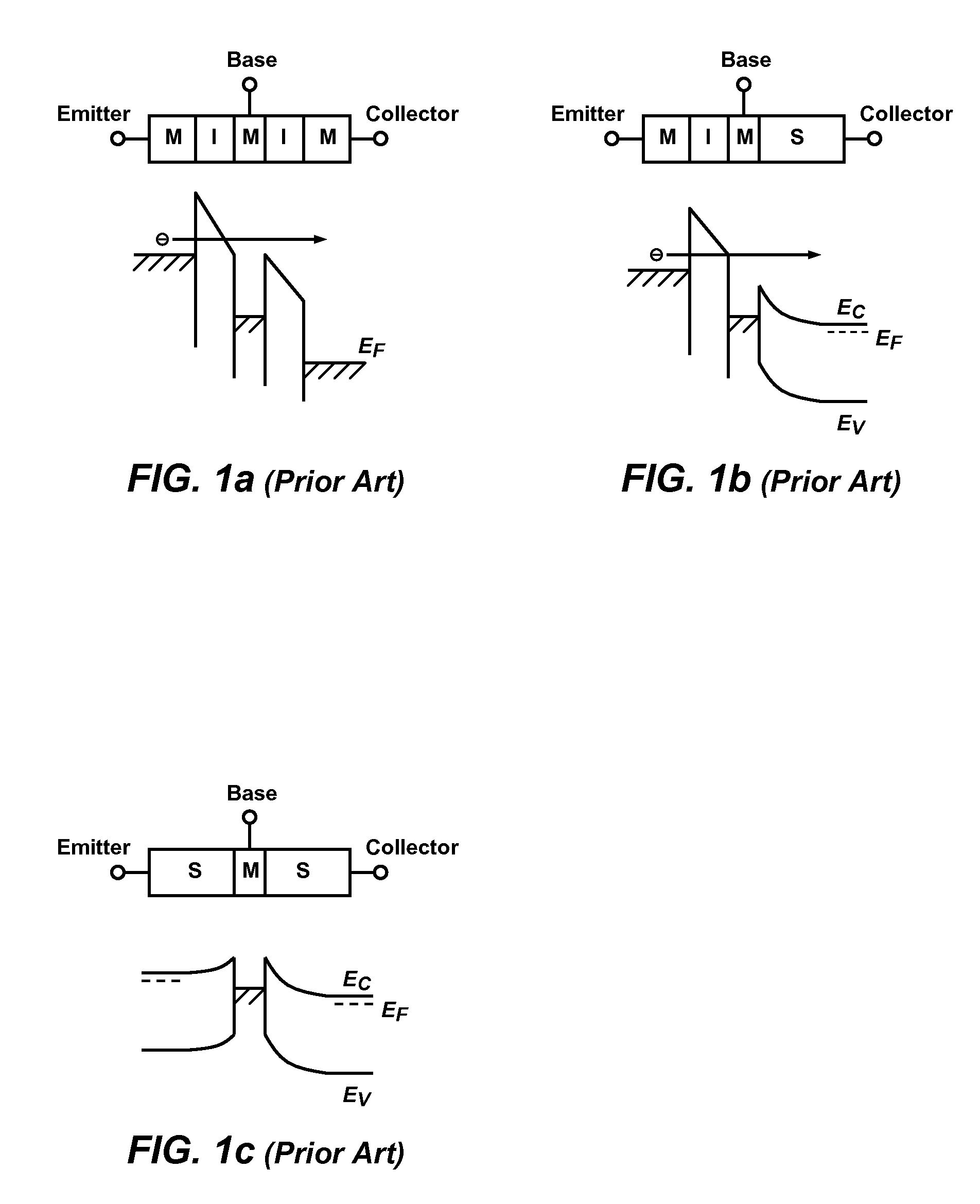
Early MBTs have been plagued by two major problems, which are the poor base transport factor αT due to their relatively large base widths and the difficulty of growth of good-quality single-crystal semiconductor materials on metals.
Because of these problems, there has been very little development on the MBT in recent years.

Method used


Image

  • Schottky barrier quantum well resonant tunneling transistor
  • Schottky barrier quantum well resonant tunneling transistor
  • Schottky barrier quantum well resonant tunneling transistor

Examples


Embodiment Construction

Ge=10, 14, and 18 ML at VB=0 V.

[0072]FIG. 14a shows hole and electron tunneling currents, Jtp and Jtn, in a p-type SBQWRTT as functions of VB for WSi,2=6, 9, and 12 ML.

[0073]FIG. 14b shows hole transmission coefficient versus energy in a p-type SBQWRTT for WSi,2=6, 9, and 12 ML.

[0074]FIG. 15a shows electron tunneling current Jtn in an n-type SBQWRTT and hole tunneling current Jtp of a p-type SBQWRTT as functions of VB for two different VC.

[0075]FIG. 15b shows Jt-VC characteristics in n-type and p-type SBQWRTTs.

[0076]FIG. 15c shows transfer curve and circuit diagram of a SBQWRTT inverter.

[0077]FIG. 16 is a top view layout of an inverter circuit consisting of one n-type SBQWRTT and one p-type SBQWRTT.

[0078]FIG. 17a is a cross-sectional view illustrating the layer structure of the SBQWRTT inverter in FIG. 16 after epitaxial growth and oxide deposition.

[0079]FIG. 17b is a cross-sectional view of the SBQWRTT inverter along the B-B′ line in FIG. 16.

[0080]FIG. 17c is a cross-sectional view...


PUM


Abstract

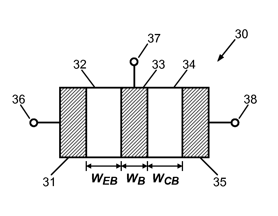
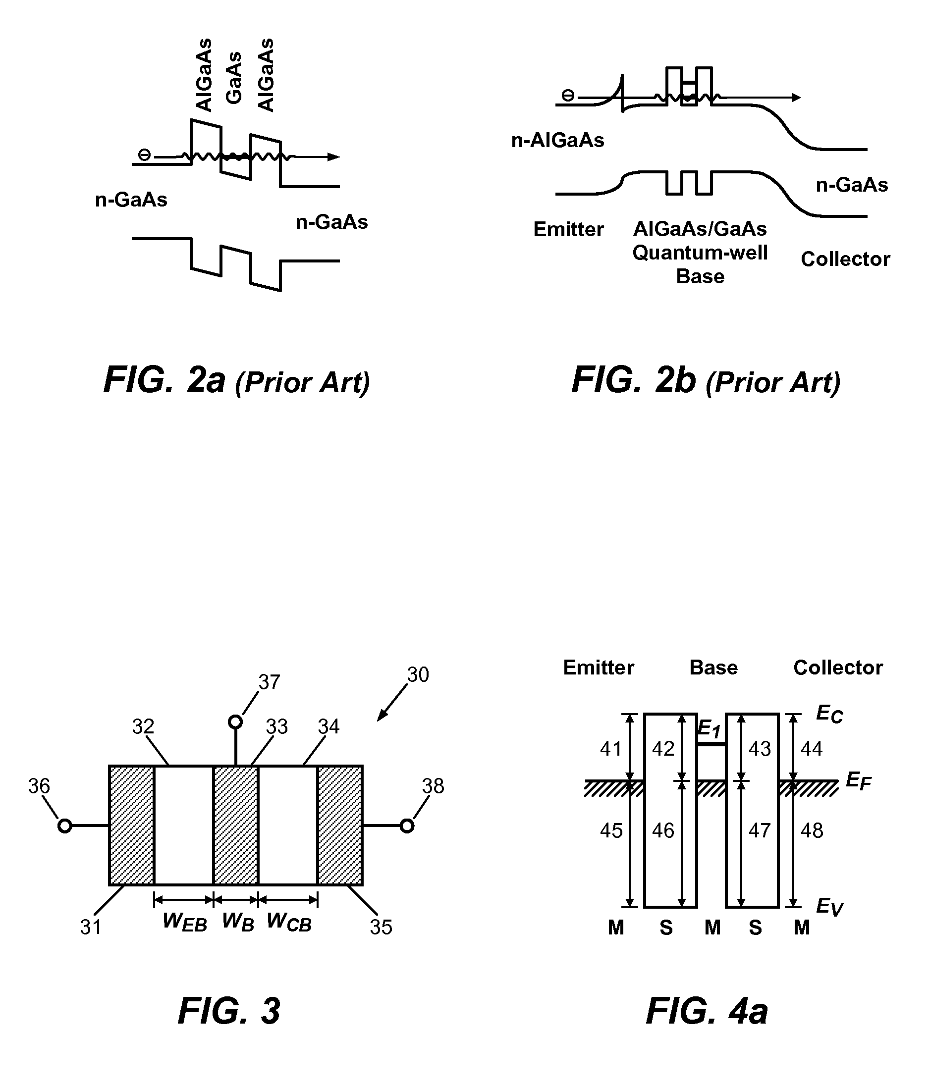
A semiconductor transistor device includes one or more conductive base regions, a first semiconductor barrier region, a second semiconductor barrier region, a conductive emitter region, and a conductive collector region. The first semiconductor barrier region or the second semiconductor barrier region has a dimension smaller than 100 Å. A first Schottky barrier junction is formed at the interface of the first semiconductor barrier region and the one or more conductive base regions. A second Schottky barrier junction is formed at the interface of the second semiconductor barrier region and the one or more conductive base regions. A third Schottky barrier junction is formed at the interface of the conductive emitter region and the first semiconductor barrier region. A fourth Schottky barrier junction is formed at the interface of the conductive collector region and the second semiconductor barrier region.

Description

TECHNICAL FIELD[0001]This application relates to a semiconductor device, specifically, a semiconductor transistor device suitable for analog and digital circuits.BACKGROUND OF THE INVENTION[0002]In the past four decades, the integrated circuit industry has followed a dramatic path of shrinking device dimensions and increasing chip sizes, resulting in steady increases of performance and functionality. New generations of devices have appeared in every two to three years, following the so-called “Moore's Law”. Each new generation has approximately reduced transistor size by 30%, increased circuit performance by about 40%, doubled logic circuit density, and quadrupled memory capacity comparing to the previous generation. The consistency of this advancement has led to an expectation that faster and more powerful chips will continue to be introduced on the same schedule in the foreseeable future.[0003]The metal oxide semiconductor field effect transistor (MOSFET) constitutes the fundament...

Claims


Application Information

Patent Timeline
Patent Type & Authority Patents(United States)
IPC IPC(8): H01L29/47
CPCH01L27/0605H01L29/0673H01L29/0676H01L29/068H01L29/7322H01L29/152H01L29/20H01L29/73H01L29/7308H01L29/0821H01L29/812
Inventor WU, KOUCHENG
Owner WU KOUCHENG
Why Eureka
Try Eureka