
Boron nitride thin-film emitter and production method thereof, and electron emitting method using boron nitride thin-film emitter

a thin-film emitter and boron nitride technology, applied in the direction of electrochemical system manufacture, solid-state diffusion coating, magnesium halides, etc., can solve the problems of difficult production methods, performance, and carbon nanotubes that have not been well established in production methods, and achieve excellent field electron emission properties

Inactive Publication Date: 2011-05-24
NAT INST FOR MATERIALS SCI
View PDF7 Cites 0 Cited by
  • Summary
  • Abstract
  • Description
  • Claims
  • Application Information

AI Technical Summary

Benefits of technology

The present invention relates to a boron nitride thin-film emitter with excellent electron emission properties, and a production method thereof. The emitter is composed of crystals that exhibit an acute-ended shape, and has a high withstand electric field strength. The invention solves the problem of limited electron emitting materials that have a high voltage endurance and a larger electric-current density, and proposes a design that takes into account the in-plane distribution density of the acute-ended crystals, which is important for achieving optimal electron emission properties. The emitter can be used in various electron emission devices such as lamps, displays, and sensors.

Problems solved by technology

However, carbon nanotubes have not been well established in production methods themselves, and still less, investigations of processing techniques therefor have been just started, thereby exhibiting an extremely difficult situation for the production methods.
Further, even by conducting such laborious and difficult processing, the obtained performance is merely limited to an electric-current density in an order of several mA / cm2 at a maximum.
This leads to a limitation of usable electric field strength of an applicable material, and exceeding the limitation causes degradation and peeling off of the material, thereby causing the material to fail to withstand usage at a higher voltage and over a long time.
However, it has gradually become apparent: that excellent electron emission properties are not sufficiently attained only by simple provision of specific shapes in design of emitter; and that extreme importance is to be given to an in-plane distribution density of acute-ended crystals.
Namely, it has become apparent that excessively higher or excessively lower crystal distribution densities rather lead to deteriorated electron emission properties, respectively.
Excessively higher densities problematically cause electric fields to fail to sufficiently permeate into the vicinity of crystals which are to emit electrons such that sufficient enhancement of electric fields are not realized near the acute ends, thereby leading to higher threshold electric fields for electron emission.
Contrary, it has gradually become apparent that excessively lower densities problematically fail to allow larger electric currents themselves.

Method used


Image

  • Boron nitride thin-film emitter and production method thereof, and electron emitting method using boron nitride thin-film emitter
  • Boron nitride thin-film emitter and production method thereof, and electron emitting method using boron nitride thin-film emitter
  • Boron nitride thin-film emitter and production method thereof, and electron emitting method using boron nitride thin-film emitter

Examples


example 1

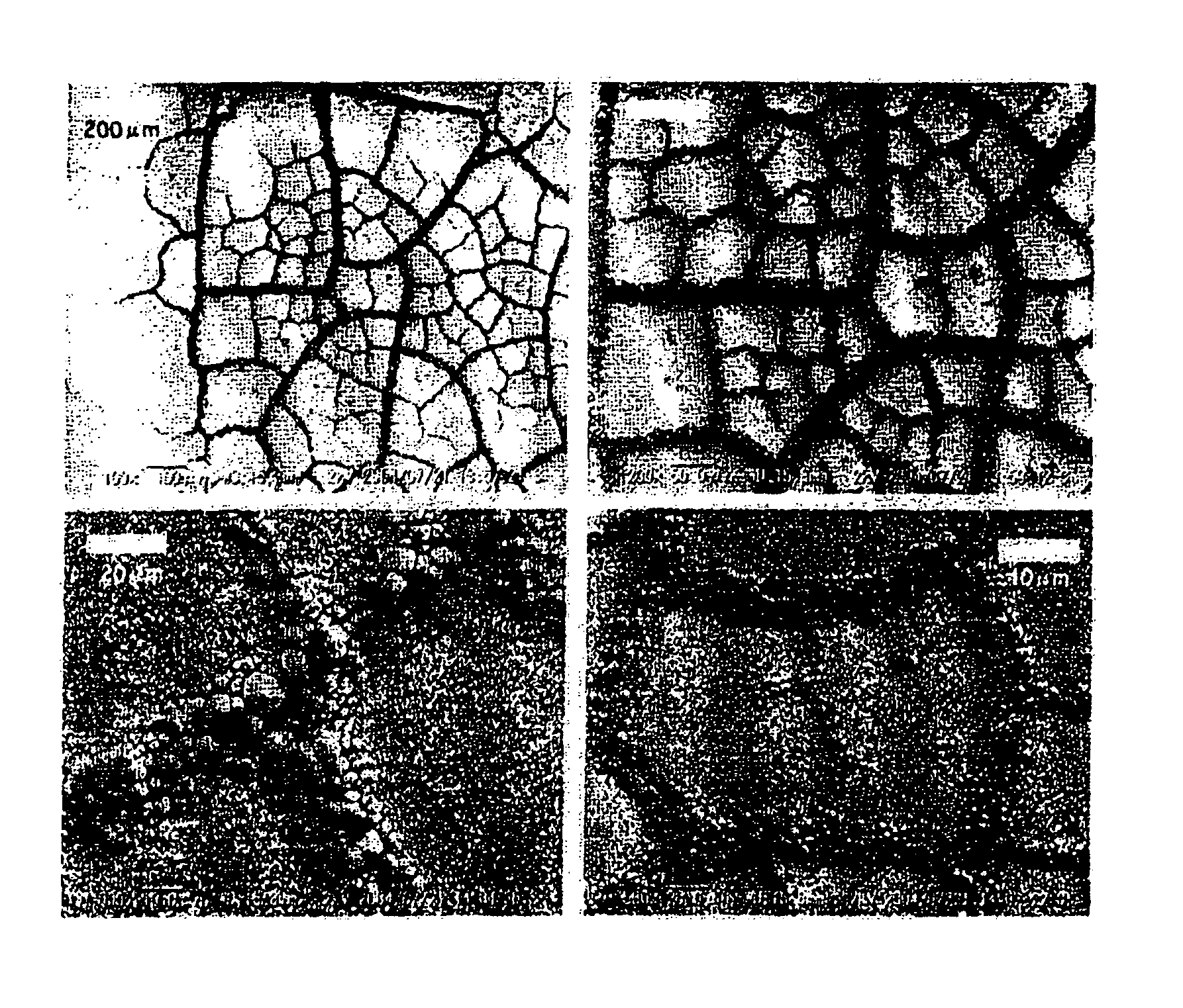
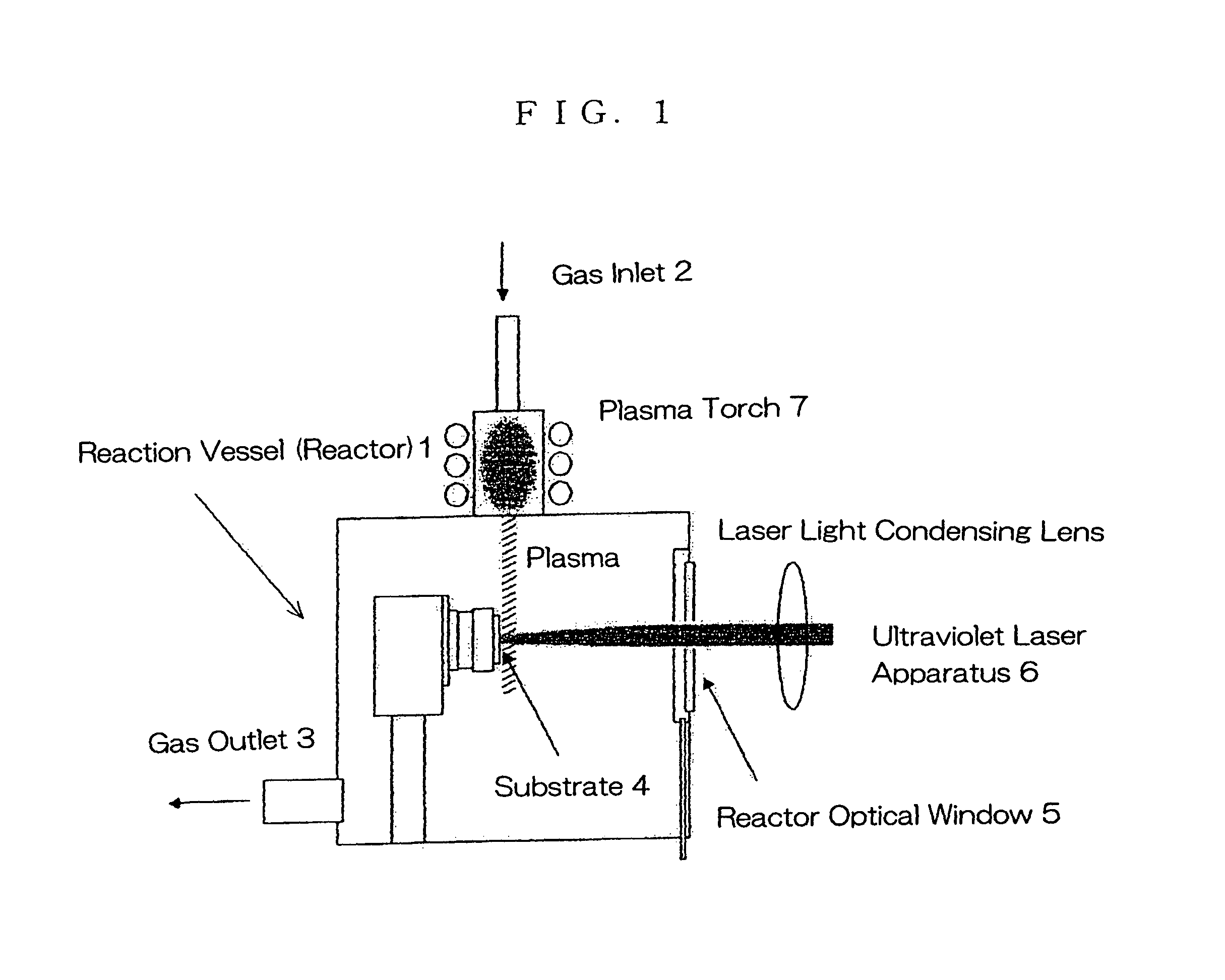
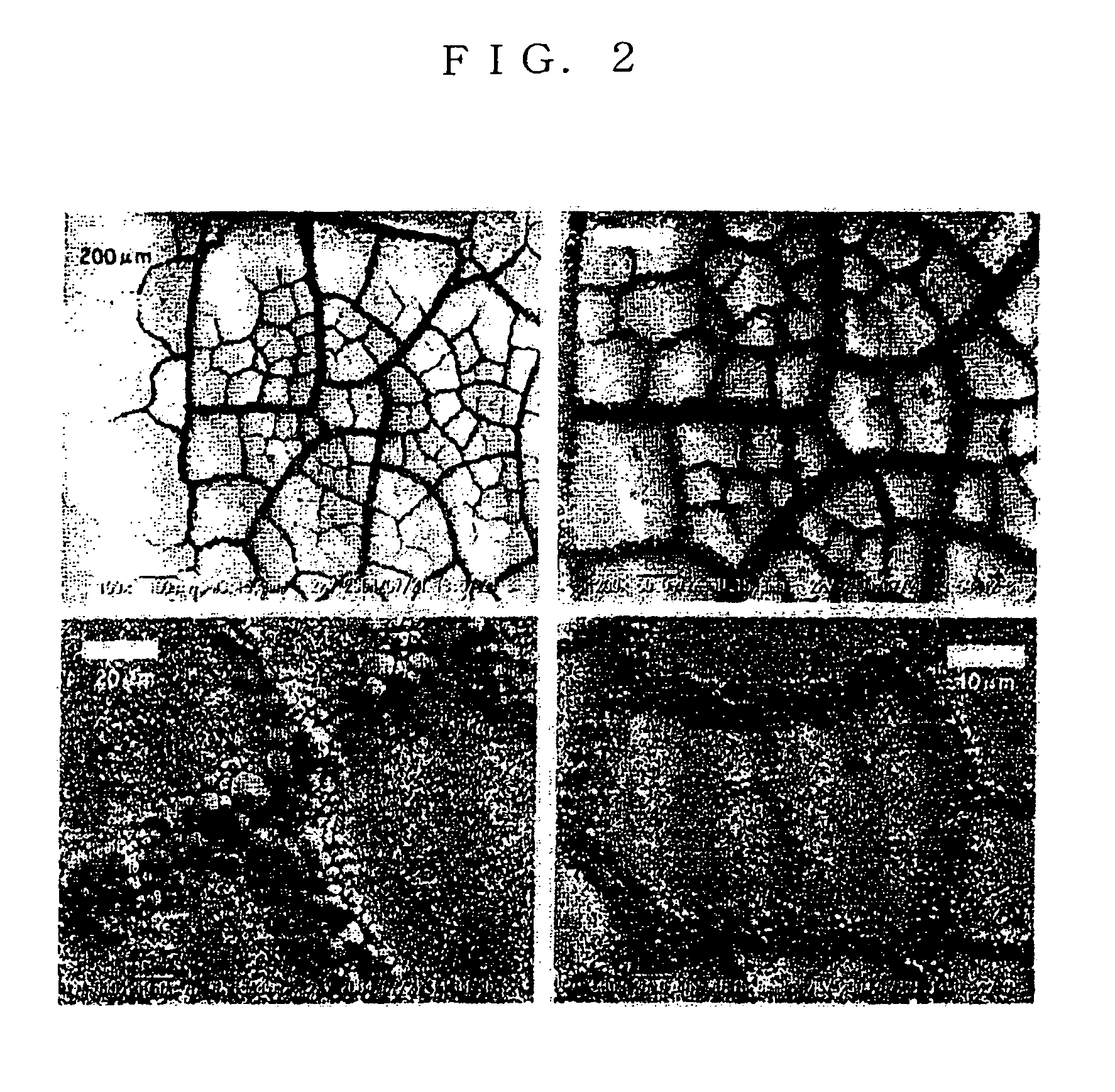
[0061]Within an ambient prepared by introducing diborane at a flow rate of 5 sccm and ammonia at a flow rate of 10 sccm into a dilution gas of argon at a flow rate of 3 SLM so that the ambient is concurrently exhausted by a pump to keep the ambient under a pressure of 10 Torr, excimer laser ultraviolet light was irradiated onto a disk-like nickel substrate having a diameter of 25 mm and kept at a temperature of 900° C. (see FIG. 1). At this time, the mixed gas was made into plasma in an inductively coupled manner by an electric field at 13.56 MHz as shown in this figure (although it has been found out that the same morphology is obtained to attain an excellent field electron emission property even when the mixed gas is not made into plasma, differences are then left in growth rate and the like). Synthesis time of 60 minutes gave an intended substance. This specimen was determined by X-ray diffraction to have a hexagonal crystal system exhibiting a 5H type polymorphic structure by sp...

example 2

[0064]As shown in FIG. 5, there were used the fractal emitter specimen obtained in Example 1, and a mica layer having a thickness of 50 μm as an inter-electrode gap forming insulation layer placed on the thin-film specimen, followed by placement of an ITO glass onto the mica layer such that an ITO surface was faced toward the specimen surface. The ITO surface acted as an anode and the specimen side acted as a cathode, while defining a gap of about 40 μm between the cathode surface and the ITO surface of anode, thereby establishing a sample for measurement of electron emission property of the emitter. Measurement method and measurement result thereof will be described in detail in Examples 3 and 4.

example 3

[0066]The fractal emitter measurement sample (see FIG. 5) obtained in Example 2 was installed in a hermetically sealed measurement vessel. At this time, placed in the vessel was a sponge containing ethyl alcohol, thereby realizing an air ambient including a large amount of ethyl alcohol and at the atmospheric pressure. Measurement results of electric current and voltage properties under this condition are shown in FIG. 6. At that time, there was connected a resistance of 100 kΩ in series with the sample, for the purpose of preventing an excessively large electric current from flowing through the sample.


PUM

PropertyMeasurementUnit
vol %aaaaaaaaaa
pressureaaaaaaaaaa
temperatureaaaaaaaaaa

Abstract

Based on designs concerning boron nitride thin-films each including boron nitride crystals in acute-ended shapes excellent in field electron emission properties, and designs of emitters adopting such thin-films, it is aimed at appropriately controlling a distribution state of such crystals to thereby provide an emitter having an excellent efficiency and thus requiring only a lower threshold electric field for electron emission.In a design of a boron nitride thin-film emitter comprising crystals that are each represented by a general formula BN, that each include sp3 bonded boron nitride, sp2 bonded boron nitride, or a mixture thereof, and that each exhibit an acute-ended shape excellent in field electron emission property; there is controlled an angle of a substrate relative to a reaction gas flow upon deposition of the emitter from a vapor phase, thereby controlling a distribution state of the crystals over a surface of the thin-film.

Description

TECHNICAL FIELD[0001]The present invention relates to a boron nitride thin-film emitter having an excellent electron emission property, comprising crystals that are each represented by a general formula BN, that each include sp3 bonded boron nitride, sp2 bonded boron nitride, or a mixture thereof, and that each exhibit an acute-ended shape excellent in field electron emission property, wherein the crystals are aggregated and distributed to exhibit a two-dimensional self-similar fractal pattern.[0002]More particularly, the present invention relates to a boron nitride thin-film emitter and a production method thereof, where the emitter is utilizable as an electron source in a lamp type light source device, a field emission type display, and the like each adopting a field emission type electron source.BACKGROUND ART[0003]In the technical field of electron emitting material, various ones have been proposed. The tendency thereof is to demand such materials each having a higher voltage en...

Claims


Application Information

Patent Timeline
Patent Type & Authority Patents(United States)
IPC IPC(8): C01B35/00H01L21/4763H05H1/24B01J19/12C01B25/00C01B21/064B05D3/00C01D3/02H01J11/04C23C14/28C23C16/00B05D3/02H01J1/304H01J9/02
CPCH01J1/304H01J9/025H01J2201/30446H01J1/30H01J9/02H01J31/12
Inventor KOMATSU, SHOJIROMORIYOSHI, YUSUKEOKADA, KATSUYUKI
Owner NAT INST FOR MATERIALS SCI
Learn More