High density micromachined electrode arrays useable for auditory nerve implants and related methods

a micromachined electrode and auditory nerve technology, applied in the field of electrical and biomedical engineering, can solve the problems of high power consumption, unable to accurately place the electrode, and the iridium wire electrodes did not permit atraumatic insertion, so as to improve the sound sensation, reduce the heat of the flip chip, and improve the effect of electrode density

Active Publication Date: 2011-08-02
RGT UNIV OF CALIFORNIA
View PDF5 Cites 85 Cited by
  • Summary
  • Abstract
  • Description
  • Claims
  • Application Information

AI Technical Summary

Benefits of technology

[0019]A flip chip assembly bonds the electrode array and the vendor fabricated electronic chip. The term “flip-chip” refers to the electronic component that is mounted directly onto another silicon substrate in a ‘face-down’ manner. Electrical connection is achieved through conductive bumps built on the surface of the chips, which is why the mounting process is ‘face-down’ in nature. During mounting, the chip is flipped on the substrate, with the bumps being precisely positioned on their target locations. Because flip chips do not require wire bonding, their size is much smaller than their conventional counterparts. Physically, the bump on a flip-chip is exactly just that—a bump formed on a bond pad of the die. Bumps serve various functions: 1) to provide an electrical connection between the die and the substrate; 2) to provide thermal conduction from the chip to the substrate, thereby helping dissipate heat from the flip chip; 3) to act as spacer for preventing electrical shorts between the die circuit and the substrate MEMS device; and 4) to provide mechanical support to the flip-chip.
[0020]In at least some embodiments of the invention, electrode arrays of the present invention may be fabricated by initially bump bonding silicon wafer to CMOS chip. Columns approximately 750 mm in height are created by bulk micromachining this silicon wafer with deep reactive ion etching (DRIE). At this height the final electrodes can penetrate to the center of the auditory nerve, thereby stimulating and recording from the maximum number of neurons. In some embodiments, columns of varying height may be formed, such that the resultant electrodes will vary in length and will thereby stimulate nerve fibers at varying depth (or in various planes) within the acoustic nerve. Since the number of stimulated neurons correlates to the fidelity of the implant, the intraneural electrode arrays of the present invention may elicit better sound sensation than current cochlear implants. Also, DRIE etching uses a photo-definable masking layer that enables a substantially higher density of electrodes than the use of dicing saws. As a result, the present invention is able to achieve more than 100 electrodes in a 1.5 square millimeter area. Each electrode may have a diameter of about 80 microns and the space between two adjacent electrodes may be about 50 microns. The columns may be sharpened into a needle shape with a two-step isotropic etching, reactive ion etching (RIE) and HNA wet etching process. The passive array may be activated by deposition of iridium to form the electrode tips and conformal coating with a layer of biocompatible Parylene C. The tips may be exposed in the final step by selectively removing Parylene C from the tip area. The surface roughness on the electrodes can be reduced by refinement of the tip-shaping process. Also, the Parylene C coating may contribute to further reduction or elimination of surface roughness.
[0021]Further in accordance with the present invention, a CMOS chip may be flip-chip bump bonded to a silicon wafer before the electrode array fabrication. The CMOS chip will have both wireless communication and DSP functions for neural recording and stimulation. This on-chip circuitry will eliminate the need for an interconnection between the electronic chip and the MEMS electrode. The most significant advantages of using wireless link and on-chip DSP instead of transcutaneous electrical wires include ease of implant surgery, vastly improved mechanical robustness, and enabling chronic implantation with minimal complications.

Problems solved by technology

This lack of spatial resolution limits the number of independent information channels that can be used to transfer auditory information through the auditory nerve to the brain.
Moreover, relatively high threshold currents are needed by the intrascalar electrodes, thus resulting in high power consumption which affects the batter life of cochlear implants.
The possibility exists to significantly improve human auditory prostheses by Simmon performed the early intranerual electrode implantations, but the relatively large size of the platinum-iridium wire electrodes did neither permit atraumatic insertion, nor accurate placement of these electrodes.
Early attempts in developing intraneural electrodes were based on platinum-iridium wire electrodes, which led to insertion trauma and reduced placement accuracy.
However, even with the use of MEMS fabrication techniques, certain issues relating to electrode size, the need for electrical wires to communicate and transfer power to the arrays, and the need for hand assembly have remained largely unsolved.

Method used


Image

  • High density micromachined electrode arrays useable for auditory nerve implants and related methods
  • High density micromachined electrode arrays useable for auditory nerve implants and related methods
  • High density micromachined electrode arrays useable for auditory nerve implants and related methods

Examples


Embodiment Construction

[0033]The following detailed description, the drawings and the above-set-forth Brief Description of the Drawings are intended to describe some, but not necessarily all, examples or embodiments of the invention. The contents of this detailed description, the accompanying drawings and the above-set-forth brief descriptions of the drawings do not limit the scope of the invention or the scope of the following claims, in any way.

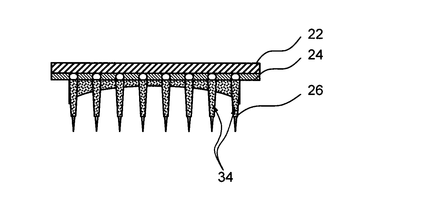
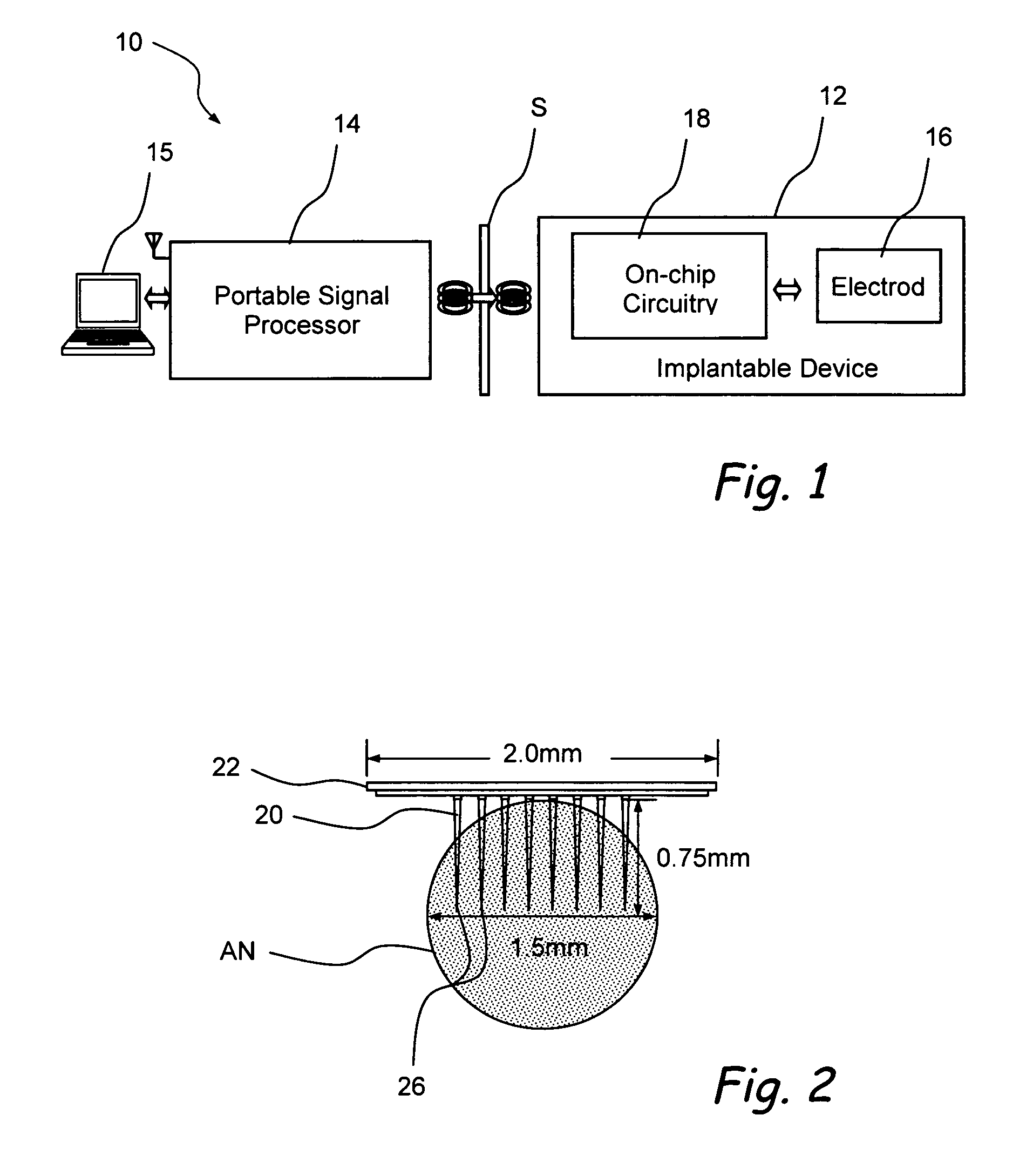
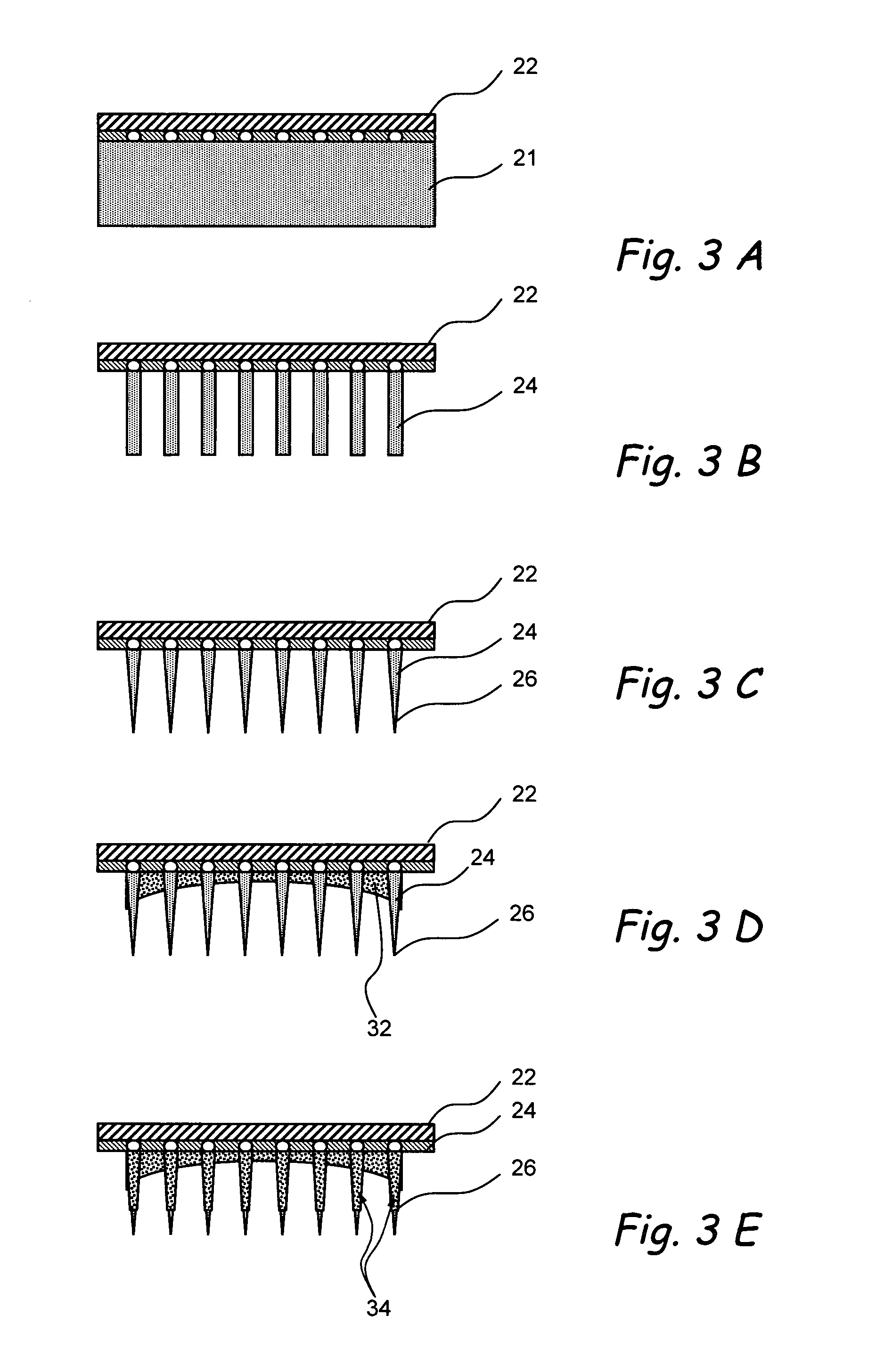
[0034]FIG. 1 is a schematic diagram of a auditory neural prosthesis system 10 comprising an implantable device 12 and a signal processor 14. The implantable device comprises an intraneural electrode array 16 with integrated on-chip circuitry 18 which can communicate in wireless fashion through the skin S with the signal processor 14. The electrode array 16 with on-chip circuitry 18 is implanted such that the electrodes of the array 16 are inserted into the auditory nerve of a human or animal subject. A bi-directional RF telemetry link is used to transfer both dat...


PUM


Abstract

Devices, systems and methods that comprise or utilize implantable electrode arrays for neural stimulation and/or sensing. In some embodiments, the electrode array is implanted or inserted into the auditory nerve and is used to deliver electrical impulses to/receive data from the auditory nerve in the treatment of hearing disorders.

Description

RELATED APPLICATION[0001]This patent application claims priority to U.S. Provisional Patent Application No. 60 / 688,982 filed Jun. 8, 2005, which is expressly incorporated herein by reference.FIELD OF THE INVENTION[0002]This invention relates generally to the fields of electrical and biomedical engineering and more particularly to implantable electrode arrays useable for neural stimulation and / or sensing.BACKGROUND[0003]The future development of advanced neuroprosthetic systems is likely to significantly improve the quality of life for persons who suffer from a variety of disorders, including those who are deaf, blind, or paralyzed, etc. Additionally, the development of apparatus and techniques for discretely sensing localized nerve impulses within neural tissue promises to provide new avenues for research and treatment of neurological disorders. However, the development of such advanced neuroprosthetic systems and sensing apparatus will be dependent upon the availability of microele...

Claims


Application Information

Patent Timeline
Patent Type & Authority Patents(United States)
IPC IPC(8): A61N1/05
CPCA61B5/04001A61B5/685A61N1/0541A61N1/36032A61B5/686A61B5/6877A61B2562/0209A61B2562/046A61B2562/125A61N1/37264A61N1/3787A61N1/36038A61B5/24
Inventor TANG, WILLIAM C.WU, JIANHAINLEY, RYAN
Owner RGT UNIV OF CALIFORNIA
Why Eureka
Try Eureka