Process for preparing conductive material

a technology of conductive materials and conductive layers, applied in the direction of photosensitive materials, conductive layers on insulating supports, instruments, etc., can solve the problems of high cost and poor productivity, inability to meet the conventional methods, and the resistance of the pattern becoming too high

Inactive Publication Date: 2011-09-06
MITSUBISHI PAPER MILLS LTD
View PDF18 Cites 40 Cited by
  • Summary
  • Abstract
  • Description
  • Claims
  • Application Information

AI Technical Summary

Benefits of technology

[0032]According to the present invention, in a preparation method which gives a conductive material having both of high transparency and high conductivity, and high storage stability, and further in a process for preparing a conductive material utilizing ultra fine silver particles, it can be provided a preparation process of obtaining a conductive material having high conductivity without requiring any calcination step which has conventionally been required.BEST MODE TO CARRY OUT THE INVENTION
[0033]The conductive material in the present invention may be mentioned, for example, conductive patterns such as fine wiring, antenna, transparent electromagnetic wave shielding film, address electrode, etc., terminals such as bump, etc., contact hole(s) or via hole(s) between wiring pattern and wiring layer(s) of a print wiring substrate comprising a plural number of layers, battery electrode(s), electrode(s) of electronic part(s), etc., but the invention is not limited by these. With regard to conductivity, electroless plating or electrolytic plating is optionally further carried out to a conductive pattern of the conductive material obtained by the present invention to strengthen the same.
[0034]The present invention is a preparation process which is to obtain a conductive material having, on a support, a conductive pattern which has high conductivity by giving conductivity to a pattern portion containing silver provided on the support, or heightening conductivity of the portion. According to the preparation processes of a pattern portion containing silver, there exist a plural number of preferred embodiments. As the first embodiment of the present invention, there is mentioned an embodiment in which a pattern portion containing silver provided on a support is a pattern portion containing silver formed by patternwisely exposing a silver salt light-sensitive material having at least one silver halide emulsion layer on the support, and then, subjecting to development. As the second embodiment of the present invention, there is mentioned an embodiment in which the pattern portion containing silver provided on the support is a pattern portion containing silver formed by providing to the support ultra fine silver particles dispersed in water and / or an organic solvent as metal colloid, but the present invention is not limited by these embodiments.
[0036]In the present invention, a metal silver image which is a pattern portion containing silver derived from a silver salt light-sensitive material is treated by a post-treatment solution containing, for example, a water-soluble halogen compound, etc., to make it a metal silver image showing a narrower value of a half-value width measured by X-ray diffraction, and as a result, to make it a metal silver image which is a conductive pattern having both of high stability and high conductivity. Accordingly, even when a post-treatment solution is acted thereon before development which forms a metal silver image, or a post-treatment solution is acted thereon by stopping the development during which an image is forming, and then subjecting to development again, etc., there is no effect but rather causes bad effects whereby conductivity cannot be obtained.
[0037]In the present invention, a silver salt light-sensitive material which is a precursor of a conductive material is, after exposure, subjected to at least one of the developing method represented by the three methods of, (1) a development according to the silver salt diffusion transfer method, (2) a development which is to fix after direct development, and (3) a development according to curing development, whereby an image is formed. The method of (1) is a method disclosed in, for example, JP 42-23745B, the method of (2) is a method disclosed in, for example, U.S. Pat. No. 6,706,165B2, and the method of (3) is a method disclosed in, for example, J. Photo. Sci. No. 11, p. 1, written by A. G. Tull (1963) or “The Theory of the Photographic Process (4th edition, p326-327)”, written by T. H. James, etc.

Problems solved by technology

However, according to these conventional methods, manufacturing processes become extremely complicated, so that they cause problems of high cost and poor productivity.
To comply with the both requirements simultaneously, it is necessary to prepare a fine metal pattern having sufficient conductivity, in particular, uniform pattern with a minimum width is required to be prepared, but this cannot be satisfied by the conventional methods.
However, when an electrolytic metal plating is to be applied to a particularly fine metal pattern, in the fine pattern, resistance of the pattern becomes too high for applying an electro-lytic plating to the fine pattern, whereby only a portion to which electricity is applied is occasionally plated.
In a conductive material using a silver salt light-sensitive photographic material as a precursor of the conductive material, a resistant material having high transparency can be prepared, but due to the problem of fluctuation of conductivity, the resistivity is deviated and the characteristics of the electromagnetic absorber is deteriorated during its preservation.
Accordingly, an object to be formed by a metal thin film is larger, a vacuum chamber which can contain such a large sized object therein is necessary, whereby there is a problem that preparation of such a material is difficult.
Also, in the preparation of a flexible printed circuits, for forming a conductive part at a concave portion such as a contact hole or a via hole, etc., there is a case of using, for example, silver paste in which silver particles having a size of 1 μm or so are mixed and kneaded in a resin, but conductivity is ensured by contact of silver particles with each other, so that there is a problem that conductivity is low.
However, for obtaining conductivity, a temperature of at least 200° C. is necessary, so that a usable substrate is limited to a heat-resistant support such as glass, polyimide, ceramic, etc.
However, even when a pattern formed by using these metal colloid solutions is sintered, a dispersant is difficultly evaporated so that the resulting conductivity was low.
Thus, to obtain good conductivity which can be used as a conductive material, it is necessary to carry out a calcination step to decompose and evaporate said dispersant, and to form mutual connection of said metal ultra fine particles due to fusion thereof, whereby not only an energy therefor is necessary but also a usable substrate is limited in the point of heat-resistance.

Method used


Image

  • Process for preparing conductive material

Examples


example 1

[0211]Examples of the first embodiment of the present invention are shown below. To prepare a precursor for the conductive material, a polyethylene terephthalate film with a thickness of 100 μm having a layer containing poly(vinylidene chloride) was used as a transparent support. Before coating a physical development nuclei layer, a base layer with a gelatin dry weight of 50 mg / m2 was coated on the film and dried. Next, a physical development nuclei layer coating solution containing palladium sulfide was prepared in the following manner.

[0212]

Solution APalladium chloride5gHydrochloric acid40mlDistilled water1000mlSolution BSodium sulfide8.6gDistilled water1000ml

Solution A and Solution B were mixed under stirring, and after 30 minutes, the mixture was passed through a column filled with an ion exchange resin to obtain palladium sulfide sol.

[0213]

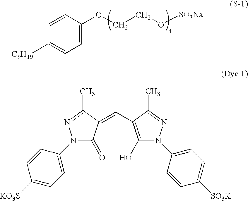
The above-mentioned palladium sulfide sol50 ml2% by weight glutaraldehyde solution20 mlSurfactant (S-1) 1 g

[0214]water was added to make up ...

example 2

[0233]By using the post-treatment solution 1-9 of Example 1, the same test was carried out in the same manner as in Example 1 except for changing the treatment temperature and treatment time. As a result, the results shown in Table 3 were obtained.

[0234]

TABLE 3SurfaceSurfaceresistanceConductiveTreatmentTreatmentresistancevalue (%)materialtemperaturetimevalueHalf-valueafterNo.(° C.)(second)(Ω / □)widthheatingRemarksB-13090500.3380PresentinventionB-24090300.3290PresentinventionB-35090300.31100PresentinventionB-46010300.3290PresentinventionB-56030200.31100PresentinventionB-66060150.3100PresentinventionB-76090150.3100PresentinventionA-15NoneNone1500.4550Comparative

[0235]From Table 3, in the case of 60° C., it can be well understood the surprising effects of the present invention that the resistance value drops⅕ of the original value with the post-treatment only for 10 seconds.

example 3

[0236]In the same manner as in Example 1, a back-coating layer was coated onto a polyethylene terephthalate film.

[0237]Subsequently, on an opposite surface of the support on which a back-coating layer has been provided, a silver halide emulsion layer 2 was coated. The silver halide emulsion was prepared by a double jet mixing method which is general in a silver halide emulsion for photography. This silver halide emulsion was so prepared that 40 mol % of silver chloride and 60 mol % of silver bromide, and an average particle size became 0.15 μm. To the thus obtained silver halide emulsion was applied a gold-sulfur sensitization using sodium thiosulfate and chloroauric acid according to the conventional manner. The thus obtained silver halide emulsion contains 1 g of gelatin per 3 g of silver.

2>

[0238]

Gelatin  1 gSilver halide emulsioncorresponding to3.0 g of silver1-Phenyl-5-mercaptotetrazole3.0 mgSurfactant (S-1) 20 mgGlyoxal (40% by weight aqueous solution) 50 mg

[0239]The thus obtai...


PUM

PropertyMeasurementUnit
temperatureaaaaaaaaaa

Abstract

It is to provide a process for preparing a conductive material in which transparency and conductivity are both high, and storage stability is high, and further, in a process for preparing a conductive material utilizing ultra fine silver particles, to provide a process for preparing a conductive material having high conductivity without requiring a calcination step which has conventionally been required.A process for preparing a conductive material having a conductive pattern containing silver on a support, which process for preparing a conductive material comprises acting at least one of the following mentioned (I) to (IV) on the pattern portion containing silver provided on the support:(I) a reducing substance,(II) a water-soluble phosphorus oxo acid compound,(III) a water-soluble halogen compound,(IV) warm water of 55° C. or higher.

Description

TECHNICAL FIELD[0001]The present invention relates to a process for preparing a conductive material having a conductive pattern containing silver on a support.BACKGROUND ART[0002]In recent years, accompanying with rapid progress of an information-oriented society, techniques regarding information-related apparatuses have rapidly been progressed and spread. Of these, a display device has been used for television, for a personal computer, for an information display at a station, airport, etc., and for providing other various kinds of information. In particular, plasma display is attracted attention in recent years.[0003]In such an information-oriented society, it has been worried about influence of an electromagnetic wave emitted by these display device. For example, it has been worried about influence on neighbouring electronic devices or influence on a human body. In particular, influence of an electromagnetic wave which exerts to health of a human body cannot ignore, and a strength...

Claims


Application Information

Patent Timeline
Patent Type & Authority Patents(United States)
IPC IPC(8): G03C1/00G03C1/005G03C5/26G03C1/06G03F7/00
CPCH05K3/106H05K2203/0786H05K2203/1157H05K2203/122H01B13/00H01B5/14H05K3/00
Inventor YOSHIKI, TAKENOBUSHINO, SHIGEKIKOBAYASHI, KAZUHISA
Owner MITSUBISHI PAPER MILLS LTD
Why Eureka
Try Eureka