All digital phase-locked loop with widely locked frequency

a phase-locked loop, all digital technology, applied in the field of phase-locked loops, can solve the problems of finite frequency resolution and quantization noise, digital and analog circuit integration, signal disturbing to the analog circuit will surely be encountered, etc., to achieve efficient transfer, shorten the locking time, and reduce the effect of process dependency

Active Publication Date: 2011-11-01
NAT TAIWAN UNIV
View PDF11 Cites 12 Cited by
  • Summary
  • Abstract
  • Description
  • Claims
  • Application Information

AI Technical Summary

Benefits of technology

[0007]In accordance with one aspect of the present invention, an all-digital phase-locked loop (ADPLL) composed of digital circuits is provided. Advantages of the new design include shorter locking time and less process dependency. The design can be efficiently transferred to different process platforms, to reduce the time consuming for system redevelopment.
[0008]In accordance with another aspect of the present invention, an all-digital phase-locked loop is provided, which is designed for the effect of a wide range of phase locking by means of adding an N-time frequency divider in front of the signal input of the ADPLL to set a frequency dividing ratio of M / N against an M-time frequency divider inside the ADPLL. As a result, the ADPLL has the advantages of higher search speed, shorter locking time, less phase jitter, and being functional on extremely high frequencies.
[0009]In accordance with a further aspect of the present invention, an ADPLL circuit architecture containing a plural number of frequency dividers is provided. Each of the frequency dividers comprises a NOR gate, three MOS components, and three tri-state inverters. Compared with the conventional static divider, the newly designed divide-by-two circuit has fewer MOS counts, less power consumption, and higher operation frequencies. Furthermore, it can be latched to either high or low arbitrarily to avoid current leakage. Therefore, the dividers are suitable for wide frequency range as well as programmable applications.
[0010]In accordance with further another aspect of the present invention, a digital controlled oscillator (DCO) comprising a plurality of tri-state inverters, a plurality of NAND gates, and a plurality of MOS components is provided, wherein eight of the MOS components are connected to four inverters. The difference in physical dimensions or size of the MOS components results in different capacitance of each component. The signal resolution in terms of the frequency of the DCO is improved by taking advantage of capacitance variations between the MOS components.
[0011]In accordance with further another aspect of the present invention, a method to operate an ADPLL composed of at least a first frequency divider, a control unit, a PFD, a DCO, a second frequency divider and a third frequency divider is provided. There are four main processes, namely the counting process, the rough tuning process, the fine tuning process, and the locked mode process. The first frequency divider divides a frequency of a feedback signal by a natural number M to generate a first output signal. The PFD generates a decrement signal and an increment signal based upon a phase difference and a frequency difference between a first reference clock signal (CKIN) and the first output signal. The control unit receives the decrement signal, the increment signal, the natural number M and a second reference clock signal (CKIN / N) to generate a plurality of digital control signals, and the digital control signals from the control unit comprise a first control signal, a second control signal, a third control signal, a first natural number N1 and a second natural number N2, and the N1 and N2 act as the divisors for the first and the second frequency dividers, respectively. The DCO generates a frequency of a clock signal (CKDCO) based upon the digital control signals. The second frequency divider receives the digital control signals from the control unit and the frequency of the clock signal (CKDCO), and divides the frequency of the clock signal by a bit number of the digital control signals to generate a feedback signal (CKOUT) to the first frequency divider. The third frequency divider divides the frequency of the first reference clock signal (CKIN) by a natural number N. In each process, the ADPLL repeatedly operates its basic functions to iterate errors until a phase difference is under an acceptable level, given that the values of the natural numbers have been pre-defined. The status of phase-locked can be achieved effectively after completion of the four processes sequentially.

Problems solved by technology

Under the stream of the system on chip (SOC) design, issues regarding the integration of digital and analog circuits such as signal disturbing to the analog circuit will sure be encountered if the traditional PLL circuit design is adopted.
Moreover, ADPLL has the problems of finite frequency resolution and quantization noise.
Unfortunately, due to a limited bandwidth (490 MHz to 1.39 GHz), outputs of the current digital controlled oscillators still cannot be broadly applied to the current wireless communication facilities (15 KHz to 1.39 GHz).

Method used


Image

  • All digital phase-locked loop with widely locked frequency
  • All digital phase-locked loop with widely locked frequency
  • All digital phase-locked loop with widely locked frequency

Examples


first embodiment

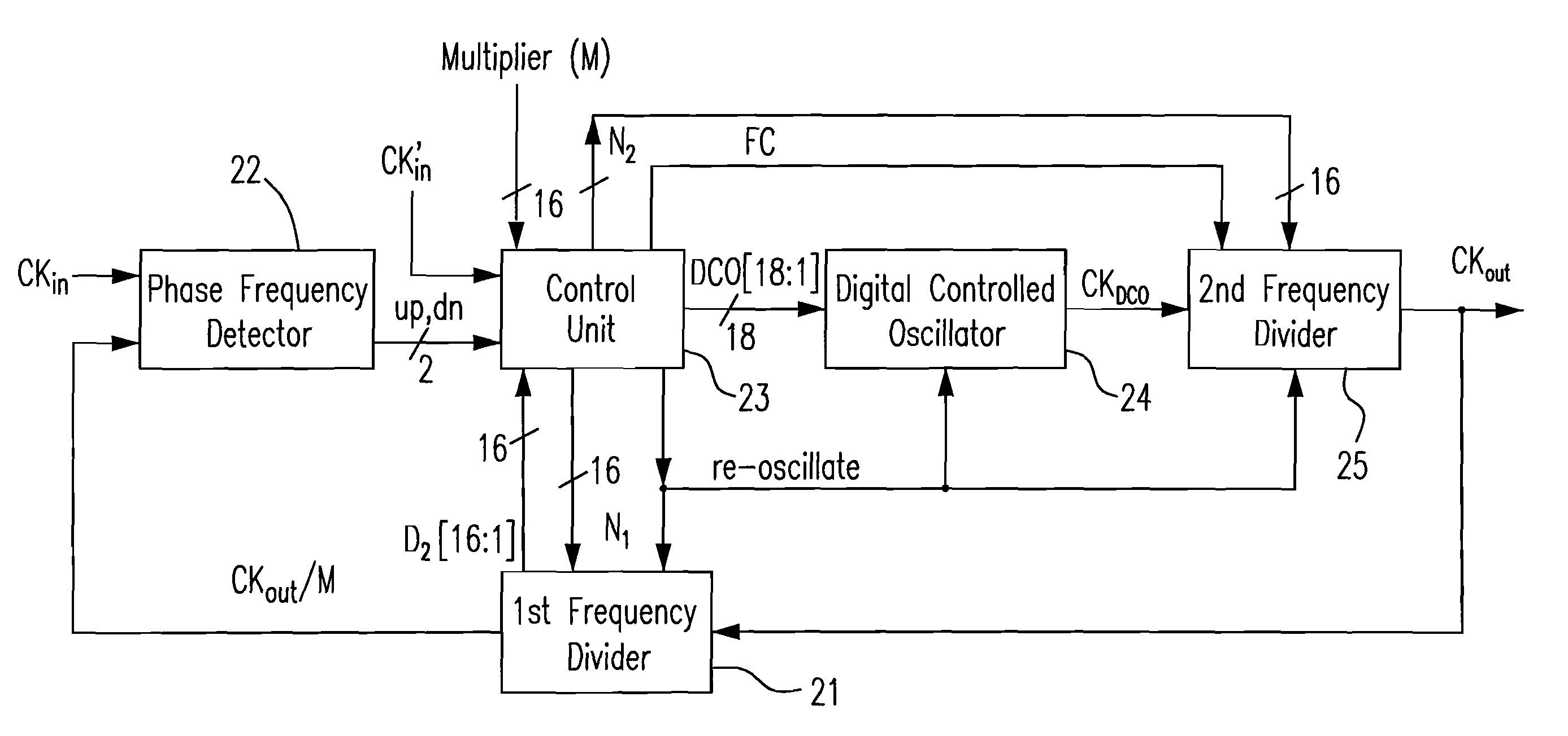
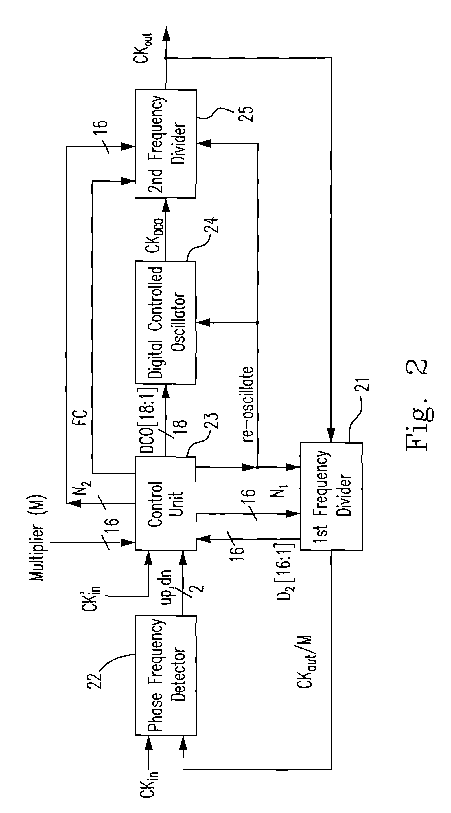
[0026]A first embodiment of the present invention is described in FIG. 2. FIG. 2 shows a circuit layout of an all-digital phase-locked loop (ADPLL) 2, wherein the ADPLL 2 is integrated into a local oscillator of an FM broadcast receiver.

[0027]According to FIG. 2, the ADPLL 2 comprises a first frequency divider 21, a phase frequency detector (PFD) 22, a control unit 23, a digital-controlled oscillator (DCO) 24, and a second frequency divider 25. The first frequency divider divides a frequency of a feedback signal CKOUT by a natural number M to reduce the frequency by M times, so as to generate a first output signal CKOUT / M. The PFD 22 generates a decrement signal dn and an increment signal up, based on a phase difference and a frequency difference between a first reference clock signal CKIN and the first output signal CKOUT / M. The control unit 23, coupled to the PFD 22, respectively receives the dn, the up, the M, and a second reference clock signal CK′IN to generate a plurality of d...

second embodiment

[0030]An advantageous embodiment for the present invention is described in FIG. 3. Based upon the first embodiment, one additional frequency divider is provided at the input terminal of the ADPLL to result in an input versus output frequency ratio of M / N where M and N are natural numbers. Please see the descriptions below.

[0031]FIG. 3 shows a circuit of the second embodiment of the present design for an ADPLL 3. In addition to a first frequency divider 31, a PFD 32, a control unit 33, a DCO 34, and a second frequency divider 35, the ADPLL 3 further comprises a third frequency divider 36 and a delay unit 37. The third frequency divider 36 is designed for producing a second output signal CKIN / N by dividing an input clock signal CKIN by a natural number N. The delay unit 37, coupled to the third frequency divider 36, delays the second output signal CKIN / N for a period of time based upon a timing difference of a level change of the second control signal re-oscillate. The delayed second ...


PUM


Abstract

An all-digital phase-locked loop (ADPLL) composed of digital circuits is provided. The ADPLL includes a phase-frequency detector (PFD), a control unit, a digital controlled oscillator (DCO), and a plurality of frequency dividers. A first frequency divider divides a frequency of a feedback signal CKOUT by a natural number M to generate a first output signal CKOUT / M. The PFD generates a decrement signal dn and an increment signal up, based on a phase difference and a frequency between a first reference clock signal CKIN and the first output signal CKOUT / M. The DCO generates a clock signal CKDCO based on the digital control signals. A second frequency divider receives the digital control signals from the control unit and the CKDCO from the DCO and divides the frequency of the CKDCO by a bit number of the digital control signals to generate a feedback signal CKOUT to the first frequency divider.

Description

FIELD OF THE INVENTION[0001]The present invention relates to a phase-locked loop, and more particularly to an all-digital phase-locked loop, for a wide range of frequencies on phase locking to electronic signals.BACKGROUND OF THE INVENTION[0002]Phase-locked loops (PLL) are widely used in telecommunications, computers and other electronic applications. With the development of the semiconductor industry, operation frequencies of microprocessors have been even higher than ever. A PLL is designed in a microprocessor as the system synchronizer as well as the frequency integrator, to eliminate any inconsistence in terms of timing between the external reference clock and internal clock, and to support the need of an internal high frequency clock. On the other hand, the PLL is much needed for system synchronizing, clock or data recovering, and frequency integration, in a communication system. PLL is important in a vast number of applications for system design.[0003]Although being widely uti...

Claims


Application Information

Patent Timeline
Patent Type & Authority Patents(United States)
IPC IPC(8): H03D3/24
CPCH03L7/091H03L7/093H03L7/0991H03L7/10H03L2207/06H03L2207/50H03L7/103
Inventor LIU, SHEN-IUANWANG, YOU-JEN
Owner NAT TAIWAN UNIV
Why Eureka
Try Eureka