Waveguide optically pre-amplified detector with passband wavelength filtering

a wavelength filtering and waveguide technology, applied in the direction of instruments, electrical equipment, lasers, etc., can solve the problems of increasing labor-intensive optical alignment, increasing the cost of volume scalability in manufacturing such components, and increasing the cost of multiple packaging, so as to reduce the impact of ase related noise on the sensitivity of the opad based receiver, the effect of enhancing the device performan

Active Publication Date: 2012-01-17
ONECHIP PHOTONICS
View PDF17 Cites 27 Cited by
  • Summary
  • Abstract
  • Description
  • Claims
  • Application Information

AI Technical Summary

Benefits of technology

[0032]The object of the invention is an integrated OPAD design, compatible with the MGVI platform, that enhances the device performance by providing on-chip ASE filtering outside the signal wavelength range and, in this manner, reducing the impact of ASE related noise on the sensitivity of the OPAD based receiver, while providing greater than e / ω receiver responsivity. The ASE filtered OPAD being formed in the MGVI platform such that, in use, the amplification and detection waveguide sections are formed within the same wavelength-designated active waveguide layer while passive waveguide sections and elements of waveguide circuitry are defined within the passive waveguide layer, the passive waveguide layer positioned below the active waveguide layer in a multi-guide vertical stack, which also may comprise other wavelength-designated active and passive waveguide layers. All elements of the MGVI photonic circuit being implemented in one epitaxial growth step and monolithically integrated on one substrate. In accordance with the MGVI design principles, see V. Tolstikhin et al in U.S. Pat. No. 7,532,784 entitled “Integrated Vertical Wavelength (De)Multiplexer” and U.S. Pat. No. 7,444,055 entitled “Integrated Optics Arrangement for Wavelength (De)Multiplexing in a Multi-Guide Vertical Stack”, the passband wavelength filter may be implemented either internally within the MGVI structure or externally to the MGVI structure.SUMMARY OF THE INVENTION

Problems solved by technology

Deep penetration of optical fiber into the access networks requires an unparalleled massive deployment of the optical interface equipment that drives the traffic to and from users.
Therefore, cost efficiency and volume scalability in manufacturing of such components are increasingly major issues.
Within a framework of the current optical component manufacturing paradigm, which is based mainly on bulk optical sub-assemblies (OSA) from off-the-shelf discrete passive and active photonic devices, the root cause of the problem lies in a labor-intensive optical alignment and costly multiple packaging.
Not only do these limit the cost efficiency, but they also significantly restrict the manufacturer's ability to ramp production volumes and provide scalability in manufacturing.
Evidently, this requirement cannot be met with any PIN photodetector, yet alone a PIN WPD, which usually has higher insertion loss and hence somewhat lower quantum efficiency than its surface illuminated counterparts.
a) electrical gain after detection, e.g. by using a phototransistor, where the signal is amplified once it is already in the electrical domain, which is not exactly a waveguide-based PIC-compatible solution and, in fact, requires an upgrade of a photonic integrated circuit (active and passive waveguide-based photonic devices integrated onto the same substrate) to an optoelectronic integrated circuit (electronic devices integrated on the same substrate with the active and passive waveguide-based photonic devices) at a cost of substantially more complicated and expensive fabrication process;
b) electrical gain in the process of detection, e.g. by utilizing an avalanche photodiode (APD), where the signal is amplified while being transformed from an optical to an electrical domain, which is fundamentally limited in terms of gain-bandwidth product, especially in its waveguide-based implementation, and for this reason is not well suited for integration into PIC for most network applications; and
c) optical gain before detection, e.g. in a semiconductor optical amplifier (SOA), where the signal is amplified without leaving the optical domain, which is a waveguide-based solution compatible with the remainder of the PIC design and fabrication processes; hereafter to be referred to as an Optically Pre-Amplified Detector (OPAD).
However, direct butt-coupling requires multiple epitaxial steps to provide the multiple semiconductor materials, which not only creates difficulty in managing optical reflections from these material interfaces, but also significantly affects the fabrication yield and thereby significantly increases the cost of the final PIC devices.
Modified butt-coupling can, potentially, remove extra epitaxial steps and in this way improve the fabrication yield, but its capabilities are limited as concerns to the semiconductor material modifications possible: usually, only the bandgap of the quantum well layer(s) can be blue shifted up to some 100 nm, whereas other layers, e.g. heavily doped contact layers, which are needed in active waveguide sections but very undesirable in the passive waveguide sections because of the propagation loss they generate, remain intact.
In contrast evanescent field coupling is free from the drawbacks of the butt-coupling approaches above, but, since it is based on the vertical rather than planar integration, it is a somewhat more complicated fabrication process based upon planar technologies, by requiring multiple etching steps at different vertical levels and creating an increased vertical topology.
If and when ASE related noise becomes the major contributor to the receiver noise, then the optical signal amplification provided by the OPAD does not help much since it worsens the signal to noise ratio and, eventually, the receiver sensitivity, in spite of increasing its responsivity.
This aspect of the OPAD performance is critical to device applications, notably in the extended reach / increased split ratio PON's, but has not been addressed properly in prior art OPAD designs.
Second, in the ASE noise limited regime, i.e. when the aggregate gain gets high, further increase of the gain has no benefit since this results in a saturation of Pmin, as can be seen from Equation (3).

Method used


Image

  • Waveguide optically pre-amplified detector with passband wavelength filtering
  • Waveguide optically pre-amplified detector with passband wavelength filtering
  • Waveguide optically pre-amplified detector with passband wavelength filtering

Examples


Embodiment Construction

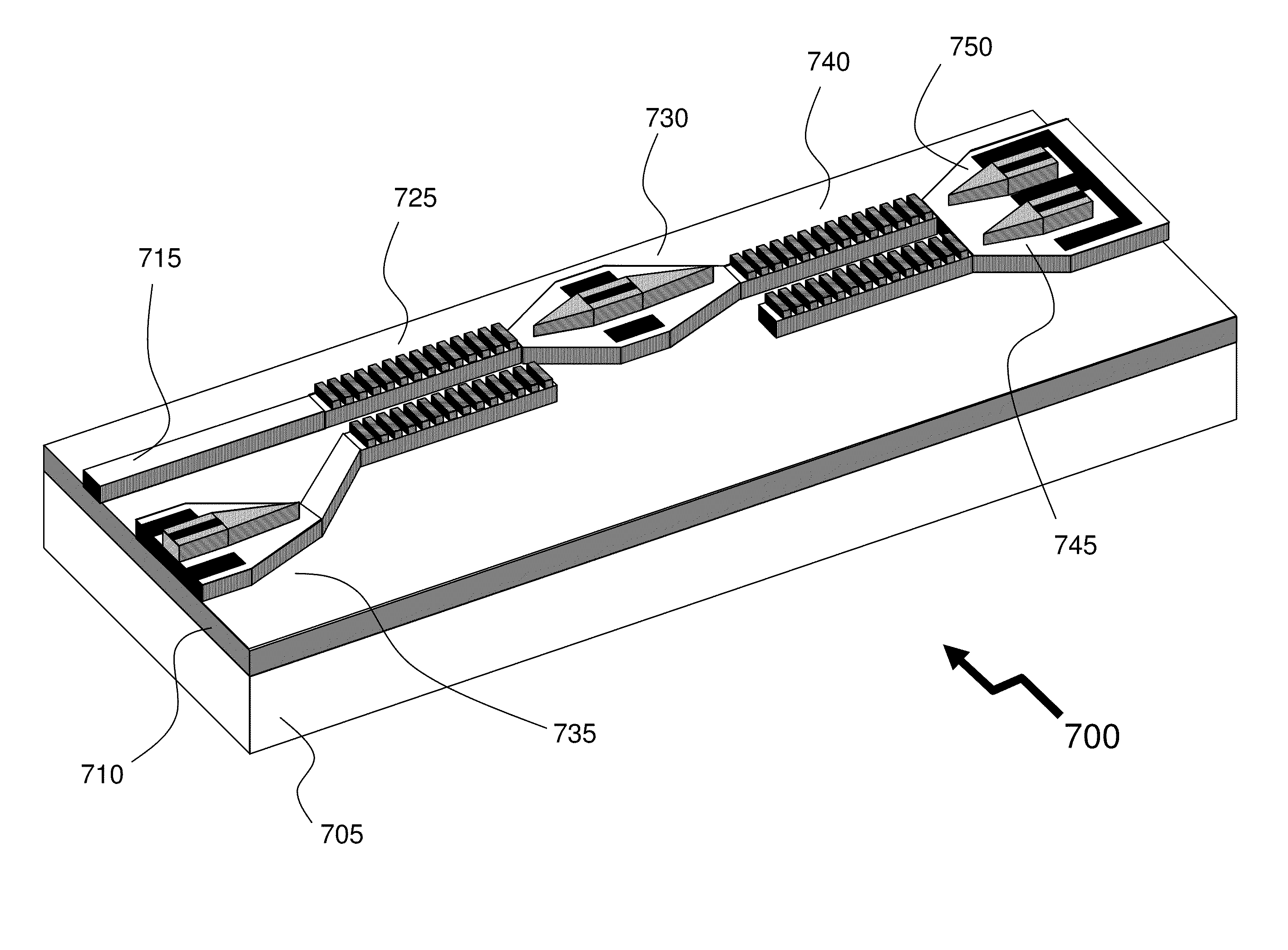
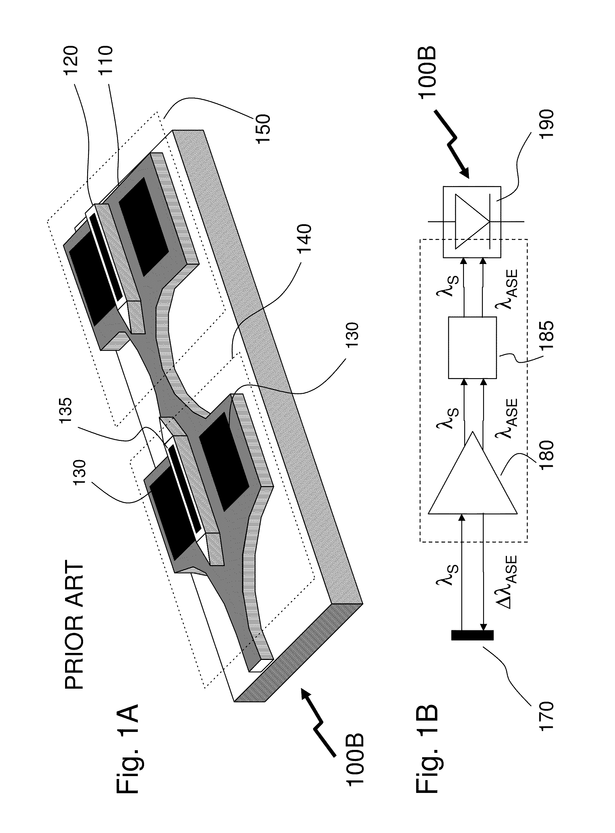
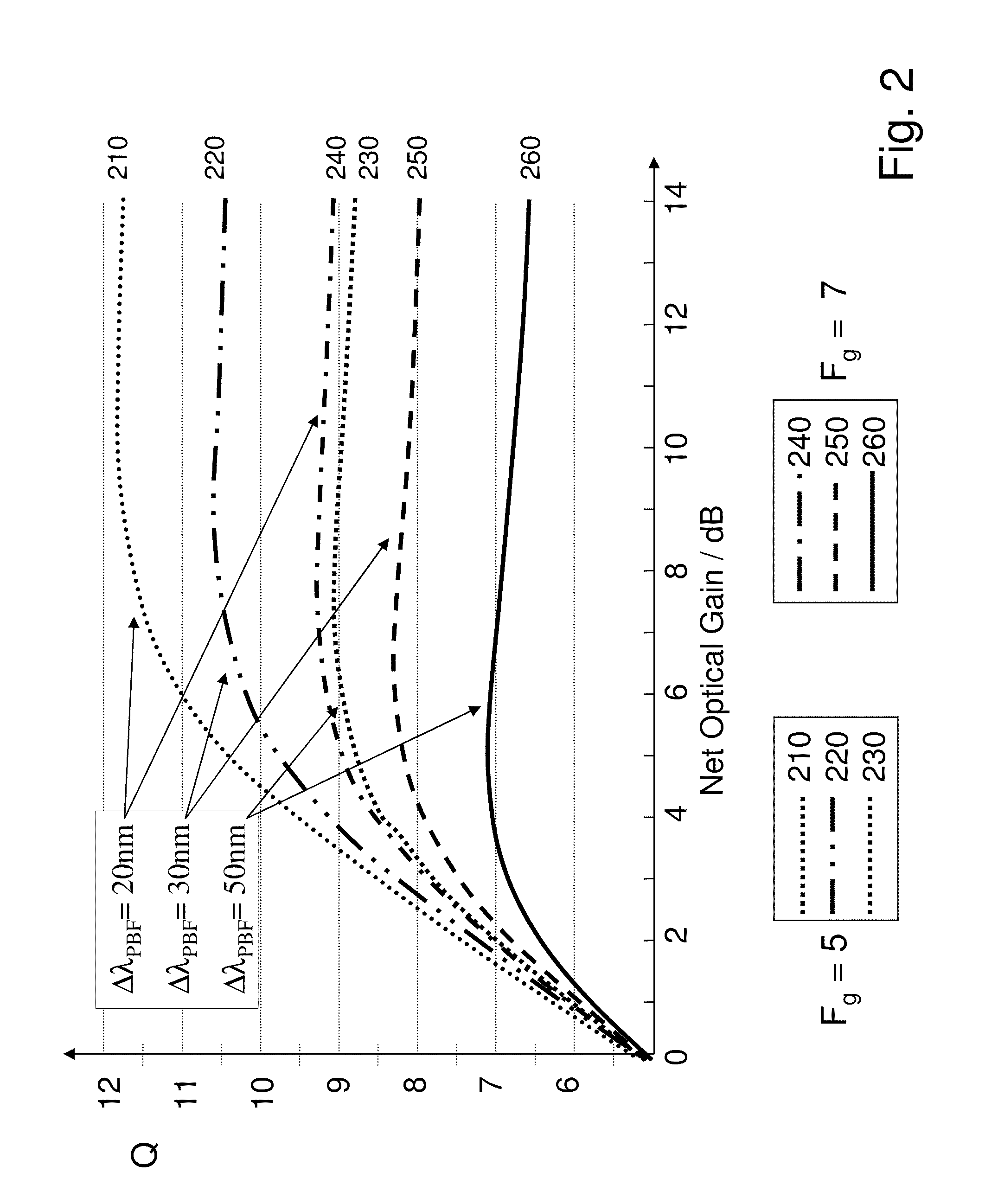
[0050]The present invention is directed to an integrated optically pre-amplified detector (OPAD) with a passband wavelength filter between amplification and detection sections of the device, which filter is intended to reduce an impact of amplified spontaneous emission generated in the amplification section of the device on broadband noise generated in the detection section of the device, thereby enhancing signal to noise ratio in and improving performance of an optical receiver featuring optically pre-amplified detector.

[0051]Reference may be made below to specific elements, numbered in accordance with the attached figures. The discussion below should be taken to be exemplary in nature, and not as limiting of the scope of the present invention. The scope of the present invention is defined in the claims, and should not be considered as limited by the implementation details described below, which as one skilled in the art will appreciate, can be modified by replacing elements with e...


PUM


Abstract

The invention describes an integrated-photonics arrangement, implementable in a multi-guide vertical integration (MGVI) structure composed from III-V semiconductors and grown in one epitaxial growth run, allowing for the integration of semiconductor optical amplifier (SOA) and PIN photodetector (PIN) structures within a common wavelength-designated waveguide of the plurality of the vertically integrated wavelength-designated waveguides forming the MGVI structure. The integration includes a wavelength filter integrated between the SOA and PIN to reduce noise within the PIN arising from ASE generated by the SOA. In exemplary embodiments of the invention, the wavelength filter is integrated into MGVI structure either within a common wavelength designated waveguide or within the wavelength-designated waveguide. Further in other embodiments the wavelength filter is provided by a thin-film filter abutting a facet of the integrated-photonics arrangement wherein optical signals are coupled by optical waveguides and / or additional optical elements such as a multimode interference device.

Description

FIELD OF THE INVENTION[0001]This invention relates to waveguide photonic devices and photonic integrated circuits and more specifically to waveguide optically pre-amplified detectors in III-V semiconductor materials.BACKGROUND OF THE INVENTION[0002]Deep penetration of optical fiber into the access networks requires an unparalleled massive deployment of the optical interface equipment that drives the traffic to and from users. For example, optical transceivers, which receive downstream signals on one wavelength and send upstream signals on another wavelength, both wavelengths sharing the same optical fiber, have to be deployed at every optical line terminal (OLT) / optical network unit (ONU). Therefore, cost efficiency and volume scalability in manufacturing of such components are increasingly major issues. It is broadly accepted within the telecommunication industry that optical access solutions are not going to become a commodity service, until volume manufacturing of the optical tra...

Claims


Application Information

Patent Timeline
Patent Type & Authority Patents(United States)
IPC IPC(8): G02B6/12
CPCH01S5/0262H01S5/5018G02B2006/12121G02B2006/12123G02B2006/12195H01S5/1014
Inventor TOLSTIKHIN, VALERYWU, FANGWATSON, CHRISTOPHERLOGVIN, YURYPIMENOV, KIRILL
Owner ONECHIP PHOTONICS
Why Eureka
Try Eureka