Methods and systems for forming thin films

a technology of thin films and systems, applied in the direction of crystal growth process, crystal growth process, crystal growth process, etc., can solve the problems of complex reactor design, limited application range, and limited application range of current methods

Inactive Publication Date: 2012-03-27
INTERMOLECULAR
View PDF73 Cites 19 Cited by
  • Summary
  • Abstract
  • Description
  • Claims
  • Application Information

AI Technical Summary

Benefits of technology

[0005]In an aspect of the invention, methods for forming Group III-V-containing thin films are provided. Methods for forming Group III-V thin films may minimize, if not eliminate, thin film contamination, thereby providing for forming high quality Group III-V thin films.

Problems solved by technology

While methods exist for forming InGaAlN films, there are limitations associated with current methods.
First, the high processing temperature involved in MOCVD may require complex reactor designs and the use of refractory materials and only materials which are inert at the high temperature of the process in the processing volume.
Second, the high temperature involved may restrict the possible substrates for InGaAlN growths to substrates which are chemically and mechanically stable at the growth temperatures and chemical environment, typically sapphire and silicon carbide substrates.
Notably, silicon substrates, which are less expensive and are available in large sizes for economic manufacturing, may be less compatible.
Third, the expense of the process gases involved as well as their poor consumption ratio, particularly in the case of ammonia, may be economically unfavorable for low cost manufacturing of InGaAlN based devices.
Fourth, the use of carbon containing precursors (e.g., trimethylgallium) may result in carbon contamination in the InGaAlN film, which may degrade the electronic and optoelectronic properties of the InGaAlN based devices.
The gas phase reactions may result in undesirable deposition of the thin film material on all surfaces within the reaction volume, and in the undesirable generation of particles.
The latter may result in a low yield of manufactured devices.
The former may result in a number of practical problems, including reducing the efficacy of in-situ optical measurements of the growing thin film due to coating of the internal optical probes and lens systems, and difficulty in maintaining a constant thermal environment over many deposition cycles as the emissivity of reactor walls will change as deposition builds up on the reactor walls.
The method may be capable of producing high quality InGaAlN thin films and devices, but the method may suffer from a tendency to form metal agglomerations, e.g., nano- to microscopic Ga droplets, on the surface of the growing film.
As such, the process may need to be carefully monitored, which may inherently result in a low yield of manufactured devices.
The method may require corrosive chemicals to be used at high temperatures, which may limit the compatible materials for reactor design.
In addition, the byproducts of the reaction are corrosive gases and solids, which may increase the need for abatement and reactor maintenance.
While the method may produce high quality GaN films at growth rates (tens to hundreds of microns per hour have been demonstrated, exceeding those commonly achieved with MOCVD), the reactor design and corrosive process inputs and outputs are drawbacks.

Method used


Image

  • Methods and systems for forming thin films
  • Methods and systems for forming thin films
  • Methods and systems for forming thin films

Examples


example

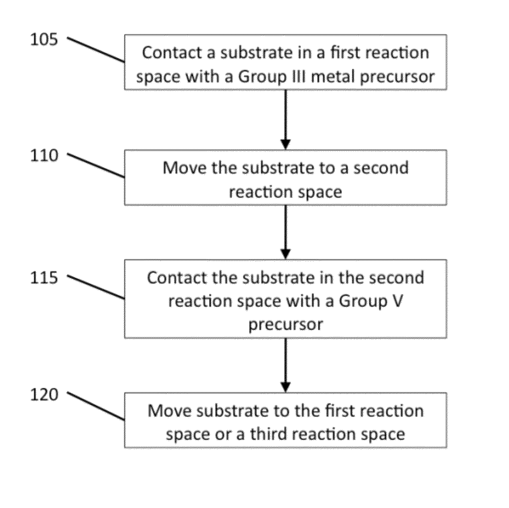
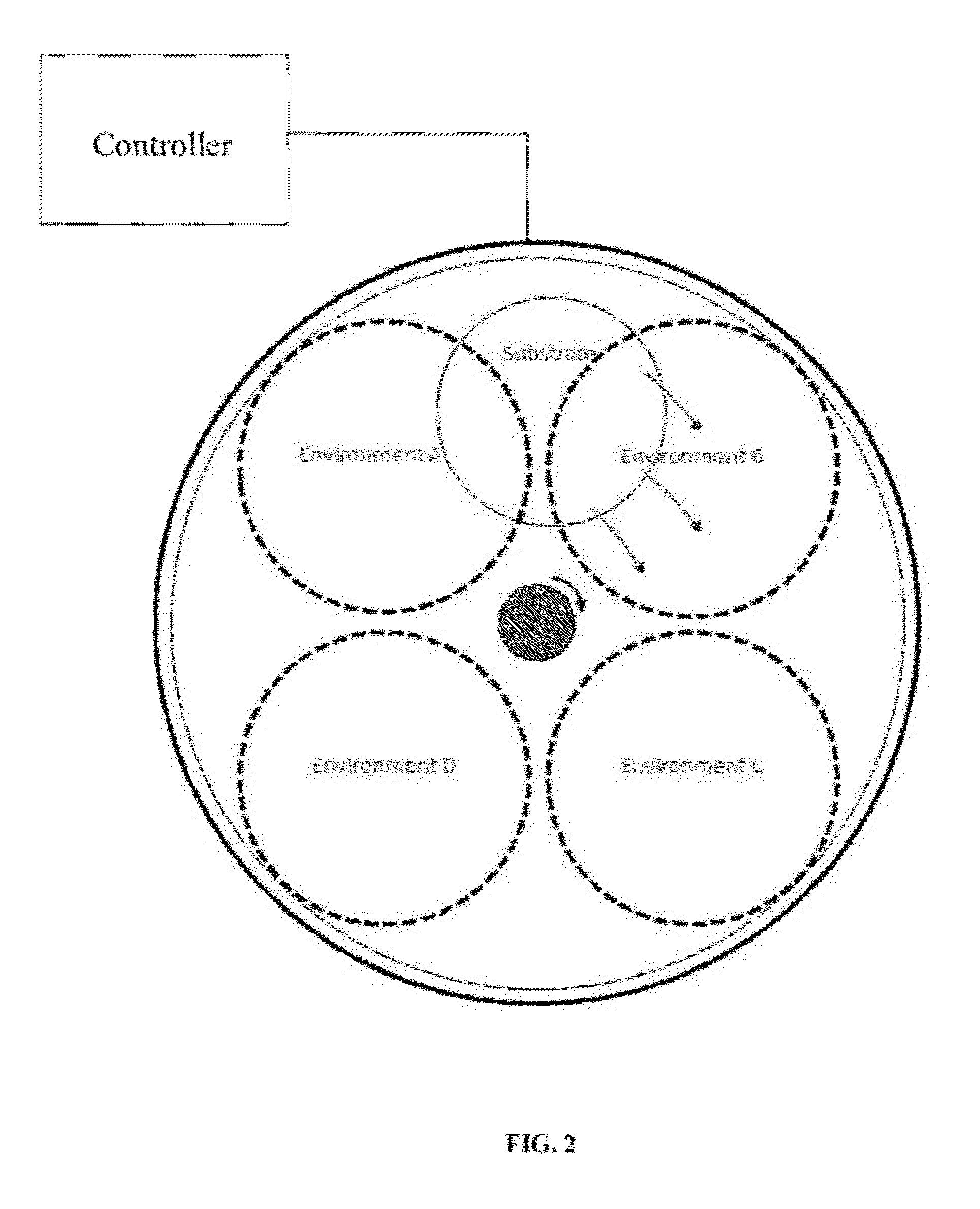
[0081]A system, such as the system of FIG. 2, includes four reaction spaces disposed in relation to one another adjacently along a circumference. A substrate, heated to a temperature of about 700° C., is provided in a first reaction space and contacted with trimethylgallium at a pressure of about 0.5 Torr. The first exposure of trimethylgallium is sufficient to form a gallium thin film at a coverage of about 0.5 ML. Next, the substrate, heated to a temperature of about 700° C., is rotated to a second reaction space and contacted with excited hydrogen-containing species, including hydrogen radicals and ions, at a pressure of about 0.5 Torr. Excited hydrogen-containing species are formed by providing plasma power of about 500 Watts to H2. Next, the substrate, heated to a temperature of about 700° C., is rotated to a third reaction space and contacted with a mixture of N2 and H2, at a pressure of about 0.5 Torr. Plasma power of about 500 Watts is provided to the mixture to generate exc...


PUM

PropertyMeasurementUnit
heightaaaaaaaaaa
root mean square of heightaaaaaaaaaa
pressureaaaaaaaaaa

Abstract

A method and apparatus for the deposition of thin films is described. In embodiments, systems and methods for epitaxial thin film formation are provided, including systems and methods for forming binary compound epitaxial thin films. Methods and systems of embodiments of the invention may be used to form direct bandgap semiconducting binary compound epitaxial thin films, such as, for example, GaN, InN and AlN, and the mixed alloys of these compounds, e.g., (In, Ga)N, (Al, Ga)N, (In, Ga, Al)N. Methods and apparatuses include a multistage deposition process and system which enables rapid repetition of sub-monolayer deposition of thin films.

Description

BACKGROUND OF THE INVENTION[0001]The growth of high-quality crystalline semiconducting thin films is a technology of significant industrial importance, with a variety of microelectronic and optoelectronic applications, including light emitting diodes and lasers. The current state-of-the-art deposition technology for gallium nitride (GaN), indium nitride (InN) and aluminum nitride (AlN) thin films, their alloys and their heterostructures (also “InGaAlN” herein) is metal-organic chemical vapor deposition (“MOCVD”), in which a substrate is held at high temperature and gases which contain the elements comprising the thin film flow over and are incorporated into the growing thin film at the surface of the wafer. In the case of GaN, the state-of-the-art may include growth temperatures of approximately 1050° C. and the simultaneous use of ammonia (NH3) and a Group III alkyl precursor gas (e.g., trimethylgallium, triethylgallium).[0002]While methods exist for forming InGaAlN films, there ar...

Claims


Application Information

Patent Timeline
Patent Type & Authority Patents(United States)
IPC IPC(8): H01L21/20
CPCC23C16/303C23C16/4554C23C16/45542C23C16/45551H01L21/0237H01L21/0254H01L21/0262H01L21/2056Y10T117/1016H01L21/205
Inventor KRAUS, PHILIP A.NIJHAWAN, SANDEEPCHUA, THAI CHENG
Owner INTERMOLECULAR
Why Eureka
Try Eureka