Semiconductor device, polycrystalline semiconductor thin film, process for producing polycrystalline semiconductor thin film, field effect transistor, and process for producing field effect transistor

a technology of semiconductor thin film and semiconductor, which is applied in the direction of semiconductor devices, basic electric elements, electrical equipment, etc., can solve the problems of difficult formation of thin film on glass substrates or organic substrates, large amount of energy and many steps, and difficult formation of thin films. , to achieve the effect of easy production, easy expansion, and reduced mobility

Active Publication Date: 2012-04-17
IDEMITSU KOSAN CO LTD
View PDF38 Cites 103 Cited by
  • Summary
  • Abstract
  • Description
  • Claims
  • Application Information

AI Technical Summary

Benefits of technology

[0147]A material for the gate insulating film 1024 is not particularly restricted, and a usually usable material can arbitrarily be selected in such a range that the effect of the invention in the present embodiment is not lost. It is possible to use an oxide such as SiO2, SiNx, Al2O3, Ta2O6, TiO2, MgO, ZrO2, CeO2, K2O, Li2O, Na2O, Rb2O, Sc2O3, Y2O3, Hf2O3, CaHfO3, PbTi3, BaTa2O6, SrTiO3 or AlN. Among them, SiO2, SiNx, Al2O3, Y2O3, Hf2O3 or CaHfO3 is preferably used, SiO2, SiNx, Y2O3, Hf2O3 or CaHfO3 is more preferably used, and Y2O3 is especially preferably used. The number of oxygen atoms of such an oxide does not necessarily have to match a stoichiometric ratio (e.g., either SiO2 or SiOx may be used).
[0148]Such a gate insulating film may have a structure in which two or more different layers of insulating films are laminated. Moreover, the gate insulating film may be crystalline, polycrystalline or amorphous, but the polycrystalline or amorphous film is preferable because it can industrially easily be produced.
[0149]Moreover, a material for the source electrode 1022 or the drain electrode 1023 is not particularly restricted, and a usually usable metal, alloy or oxide conductor material can arbitrarily be selected in such a range that the effect of the invention in the present embodiment is not lost.
[0150]Next, a process for producing the polycrystalline oxide semiconductor thin film 1002 used in the thin-film transistor 1001 will be described.
[0151]When the polycrystalline oxide semiconductor thin film 1002 is formed, as a sputtering process, there may be utilized a DC sputtering process, a DC magnetron sputtering process, an AC sputtering process, an AC magnetron sputtering process, an RF sputtering process, an RF magnetron sputtering process, a facing target sputtering process, a cylindrical target sputtering process, an ECR sputtering process or the like. Moreover, as a vacuum deposition process, a resistance heating process, an electron beam heating process, a pulse laser deposition (PLD) process or the like may be utilized. Furthermore, as an ion plating process, an ARE process or an HDPE process may be utilized. In addition, as a CVD process, a heat CVD process or a plasma CVD process may be utilized.
[0152]Among them, the DC magnetron sputtering process in which discharge is stabilized and which is inexpensive and can easily be enlarged, or the AC magnetron sputtering process is industrially preferable. The DC magnetron sputtering process is especially preferable. Moreover, a co-sputtering process, a reactive sputtering process or a DC / RF superimposition sputtering process may be utilized.

Problems solved by technology

Furthermore, in the case of a crystalline silicon-based thin film, a high temperature of, for example, 800° C. or more is required at its crystallization, and hence it is difficult to form the thin film on a glass substrate or an organic substrate.
Therefore, the formation of the thin film is possible only on an expensive substrate such as a silicon wafer or quartz having a high heat resistance.
In addition, for the production of the film, a large amount of energy and many steps are necessary.
Furthermore, in the crystalline silicon-based thin film, the element constitution of the TFT is usually limited to a top gate constitution, and hence it has been difficult to decrease the number of masks or the like, which disturbs the decrease of production costs.
Therefore, when the amorphous silicon is used as the switching element for driving the display device, such an element cannot follow up the display of a dynamic image at a high speed on occasion.
Furthermore, when a semiconductor active layer is irradiated with visible light, the layer exerts conductivity, and a leakage current might be generated to cause malfunctions.
Thus, properties as the switching element deteriorate on occasion.
Therefore, the light block layer needs to be set to a ground level, and also in this case, a parasitic capacity is generated.

Method used


Image

  • Semiconductor device, polycrystalline semiconductor thin film, process for producing polycrystalline semiconductor thin film, field effect transistor, and process for producing field effect transistor
  • Semiconductor device, polycrystalline semiconductor thin film, process for producing polycrystalline semiconductor thin film, field effect transistor, and process for producing field effect transistor
  • Semiconductor device, polycrystalline semiconductor thin film, process for producing polycrystalline semiconductor thin film, field effect transistor, and process for producing field effect transistor

Examples


example 1

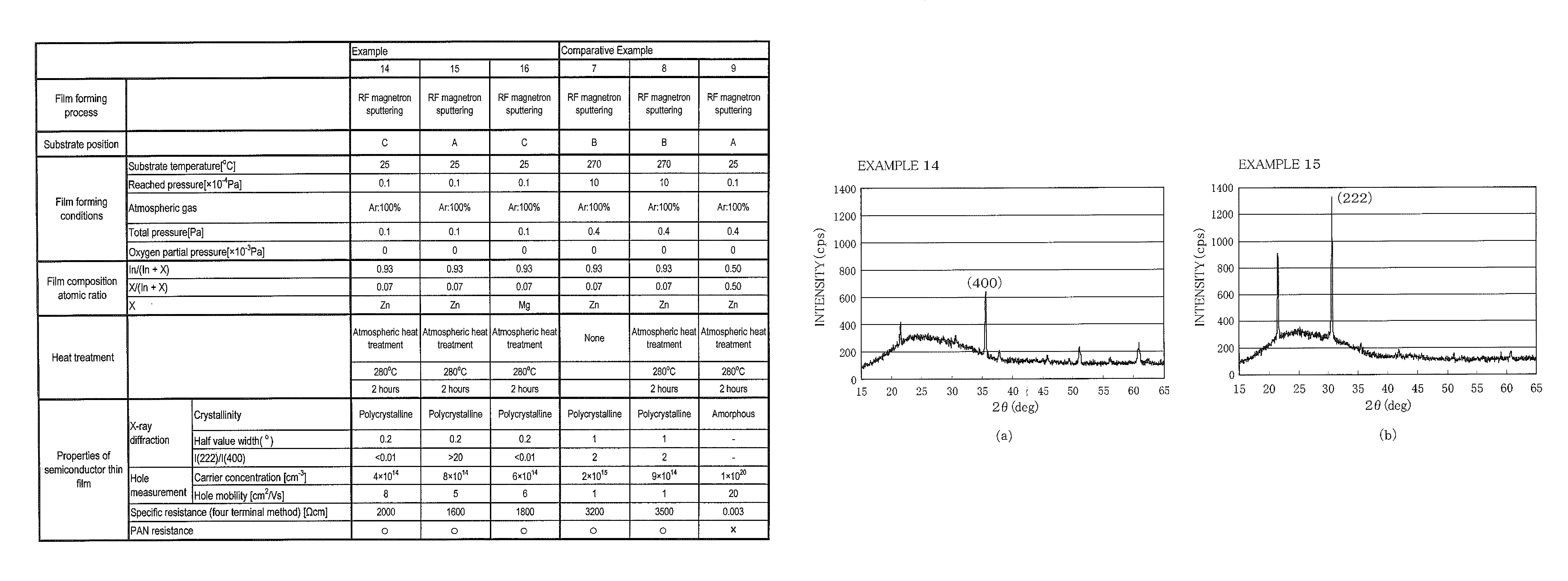
[0174]FIG. 4 is a table showing a film forming process, film forming conditions, a film composition atomic ratio, an oxidation treatment and the properties of a semiconductor thin film in Examples 1 to 13 and Comparative Examples 1 to 6.

[0175]Production Example of Crystalline Oxide

[0176](1) Production of Sputtering Target

[0177]As raw materials, powders of indium oxide, zinc oxide and magnesium oxide were mixed so that an atomic ratio [In] / ([In]+[Zn]+[Mg]) was 0.93, an atomic ratio [Zn] / ([In]+[Zn]+[Mg]) was 0.06 and an atomic ratio [Mg] / ([In]+[Zn]+[Mg]) was 0.01, and the resultant mixture was fed to a wet-type ball mill, mixed and ground for 72 hours to obtain a fine material powder.

[0178]The obtained fine material powder was granulated, and then the resultant granules were pressed into a dimension with a diameter of 10 cm and a thickness of 5 mm. The pressed material was placed in a firing furnace, and fired under conditions at 1450° C. for 12 hours to obtain a sintered article (the...

example 2

[0207]An oxide of Example 2 was produced under about the same producing conditions (a film forming process, film forming conditions, a film composition atomic ratio and an oxidation treatment) as in Example 1 except that Cu was added instead of Mg.

[0208]With regard to the properties of the oxide produced under the above producing conditions, as shown in FIG. 4, a crystallinity was polycrystalline, a carrier concentration was about 3×1014 cm−3, and a Hall mobility was about 5 cm2 / Vs. The value of a specific resistance measured by a four terminal method was about 1100 Ωcm. Furthermore, an energy band gap was about 3.2 eV, and PAN resistance and heat resistance were denoted by o in the table, respectively. As transistor properties, though not shown in the drawing, a mobility was 80 cm2 / Vs, and an on-off ratio was 107 or more.

[0209]That is, the polycrystallized oxide of Example 2 described above had properties as an excellent transparent semiconductor thin film. Moreover, a thin-film tr...

example 3

[0210]An oxide of Example 3 was produced under about the same producing conditions (a film forming process, film forming conditions, a film composition atomic ratio and an oxidation treatment) as in Example 1 except that Ni was added instead of Mg.

[0211]With regard to the properties of the oxide produced under the above producing conditions, as shown in FIG. 4, a crystallinity was polycrystalline, a carrier concentration was about 3×1014 cm−3, and a Hall mobility was about 5 cm2Vs. The value of a specific resistance measured by a four terminal method was about 1100 Ωcm. Furthermore, an energy band gap was about 3.2 eV, and PAN resistance and heat resistance were denoted by o in the table, respectively. As transistor properties, though not shown in the drawing, a mobility was 80 cm2 / Vs, and an on-off ratio was 107 or more.

[0212]That is, the polycrystallized oxide of Example 3 described above had properties as an excellent transparent semiconductor thin film. Moreover, a thin-film tra...


PUM


Abstract

An object of the present invention is to provide a novel semiconductor device which is excellent in stability, uniformity, reproducibility, heat resistance, durability and the like, and can exert excellent transistor properties. The semiconductor device is a thin-film transistor, and this thin-film transistor uses, as an active layer, a polycrystalline oxide semiconductor thin film containing In and two or more metals other than In and having an electron carrier concentration of less than 1×10¹⁸ / cm3.

Description

TECHNICAL FIELD[0001]The present invention relates to a semiconductor device, a polycrystalline semiconductor thin film, a process for producing a polycrystalline semiconductor thin film, a field effect transistor, and a process for producing a field effect transistor.[0002]In particular, the present invention relates to a semiconductor device which uses, as a semiconductor, a crystalline oxide containing In and two or more metals other than In and having a predetermined electron carrier concentration. Moreover, the present invention relates to a polycrystalline semiconductor thin film having a high crystallinity and including crystals aligned in a predetermined direction, a process for producing the polycrystalline semiconductor thin film, a field effect transistor, and a process for producing the field effect transistor.BACKGROUND ART[0003]Field effect transistors are broadly used as unit electron elements of semiconductor memory integrated circuits, high-frequency signal amplific...

Claims


Application Information

Patent Timeline
Patent Type & Authority Patents(United States)
IPC IPC(8): H01L29/12
CPCH01L29/7869
Inventor YANO, KOKIINOUE, KAZUYOSHI
Owner IDEMITSU KOSAN CO LTD
Why Eureka
Try Eureka