Optical devices and digital laser method for writing waveguides, gratings, and integrated optical circuits

a technology of optical devices and lasers, applied in the field of optical devices and digital lasers, can solve the problems of inflexible method in comparison with holographic method, weak reflection of bragg gratings formed in planar lightwave circuits, and relatively slow point-by-point fabrication method, etc., to achieve short period of time, reduce cost, and simplify the effect of fabrication process

Active Publication Date: 2012-09-18
HERMAN +1
View PDF7 Cites 24 Cited by
  • Summary
  • Abstract
  • Description
  • Claims
  • Application Information

AI Technical Summary

Benefits of technology

[0028]In an embodiment of the present invention, a pulsed laser is used to alter the refractive index of a transparent material and create a periodic structure therein. By controlling the scan speed during laser writing and optimizing the laser exposure parameters, isolated or near-isolated laser-modified volumes can be formed in the transparent material with arbitrary periodic spacing that (i) define a low loss optical waveguide that can be scanned flexibly in any 3D path through the media, and (ii) simultaneously superimpose a periodic or chirped grating that provides a controlled spectral response for reflection, diffraction, and / or transmission within any section of the waveguide. The grating periods can be varied to form highly complex optical circuits in relatively short period of time. The method also provides for apodization and aperiodic chirping of the grating structures by various means, for example, by tuning the relative scanning speed or the laser intensity during the point-by-point fabrication.
[0029]Advantageously, the method of the present invention enables 3D fabrication and integration of sensing and filtering functions in 1D, 2D, and 3D optical circuits. Because only one laser writing step can be employed, the method of the present invention simplifies the fabrication process which leads to lower cost and enables highly versatile optical devices or systems to be designed and fabricated.

Problems solved by technology

As well, a point-by-point method is a relatively slow fabrication method, is generally directed to coarse (long period) structures, and requires an existing waveguide and a mask.
However, this method is inflexible in comparison with the holographic method, for example, when multiple wavelength Bragg grating devices are required.
Separate generally high-cost phase masks are required for each Bragg wavelength, and relatively time-consuming multiple laser exposures with various the phase masks are then necessary to produce the desired multi-wavelength spectral response.
The technique has a disadvantage over the formation of FBGs in that Bragg gratings formed in planar lightwave circuits have weaker reflection due to lower photosensitivity of glass materials contained in the planar light circuit.
However, a roadblock in the development of such 3D laser writing processes has been the inability to generate basic grating filter / reflectors devices within the 3D waveguide structures formed by the laser writing method.
However, this technique has only been demonstrated to be successful in a pre-existing waveguide (optical fiber).
However, this point-by-point method only provides low spatial modulation and therefore is very limited in the type of gratings that can be formed.
The basic grating fabrication techniques, including (i) the use of amplitude / phase masks, (ii) holographic interference of two beams, and (iii) point-by-point grating writing, suffer from numerous disadvantages, including being expensive, time-consuming, and not readily applicable to 3D application.

Method used


Image

  • Optical devices and digital laser method for writing waveguides, gratings, and integrated optical circuits
  • Optical devices and digital laser method for writing waveguides, gratings, and integrated optical circuits
  • Optical devices and digital laser method for writing waveguides, gratings, and integrated optical circuits

Examples


example 1

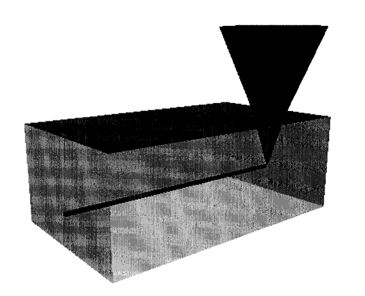
[0071]FIG. 2 depicts a laser writing arrangement in accordance with one example embodiment of the present invention. The laser is delivered to the sample by mirrors and a focusing lens. In this embodiment, the sample is mounted on a two-axis motion stage for horizontal scanning in x or y direction while a vertical motion stage positions the lens to focus the beam at a controlled depth below the surface of the material where modification is confined inside or nearby the laser focal volume.

[0072]In this particular embodiment of the present invention, a pulsed ultrashort (1) is used to deliver 1 kHz pulses with 35 fs minimum duration and 2.5 mJ maximum per pulse energy. The laser beam was relayed to a granite structure (2) in which a 3D air-bearing motion stage system (2) is mounted. The beam coming from the Z direction (optical axis) was then focused by a 0.25NA aspherical lens (4) to ˜200 μm below the surface of a glass sample (Corning EAGLE2000™) (5) of 50×50×1 mm3 size which is fix...

example 2

[0085]GW structures were fabricated by partial or non-overlapping pulses of the same 1 kHz ultrashort laser in fused silica glasses. When focused by a 0.25 NA aspherical lens and scanned with ˜1 mm / s velocity relative to the bulk fused silica glass (50×50×1 mm3), the pulsed laser produced low loss (minimum ˜0.2 dB / cm) waveguides for guiding visible light (633 nm wavelength). The GW structures are similar to the GW structures discussed in example 1 above. However, the laser interaction processes for fused silica are distinguishable in one aspect: the GW structure made in fused silica glass can guide visible wavelength with very low loss compared with the low loss infrared-guiding behaviour in the example above. Further, an examination of a wide 50 fs to 5 ps range of laser pulse duration shows the lowest loss waveguides to form in a narrow 1.0±0.2 ps window. This low-loss processing window has not been previously reported and such relatively long pulse duration significantly exceeds ...

example 3

[0098]Laser exposure conditions were optimized and tighter focusing and longer duration laser pulses led to improved grating strength and reduced waveguide propagation loss. The same 1 kHz Ti:Sapphire ultrafast laser system (Spectra Physics™ Spitfire Pro) delivered 2.4 mJ maximum energy at 800 nm wavelength. The laser pulse duration was tuned from 100 fs to 2 ps by adjusting the laser compressor grating. A tighter 0.55 NA aspheric lens was used to focus the laser beam to ˜1 μm diameter (1 / e2 intensity) at a position 200 μm below the surface of a borosilicate glass sample (Corning EAGLE2000™, 50 mm×10 mm×1 mm). The glass sample was mounted on 3D air-bearing motion stages (Aerotech™ ABL1000, 2 nm resolution and 50 nm repeatability) and scanned transverse to the laser direction to produce 10 mm long grating waveguides. Sample scan speed was fixed at 0.52 mm / s to yield 1st-order Bragg reflection at 1550 nm for the 1 kHz laser repetition rate. The laser energy was adjusted from 0.5 to 10...


PUM

PropertyMeasurementUnit
pulse energyaaaaaaaaaa
scanning speedaaaaaaaaaa
scan velocitiesaaaaaaaaaa

Abstract

The invention relates to devices having periodic refractive index modulation structures and fabrication methods for the devices using a laser means. By focusing a pulsed laser beam into a transparent material substrate, a path of laser modified volumes can be formed with modified refractive index compared with the unprocessed material. By selecting appropriate laser parameters and relative scan speed, the laser modified path defines an optical waveguide. Separation distance of the individual modified volumes define a periodic modification pattern along the waveguide path, so that the waveguide structures also exhibit grating responses, for example, as spectral filters, Bragg reflectors, grating couplers, grating sensors, or other devices. This method of direct laser fabrication enables one-step fabrication and integration of periodic or aperiodic refractive-index modulation devices together with optical waveguiding properties to enable low-cost, multifunctional 1D, 2D or 3D optical circuit fabrication for simple and complex applications.

Description

PRIORITY[0001]This application claims the benefit of U.S. Provisional Patent Application No. 60 / 801,386, filed on 19 May 2006.FIELD OF THE INVENTION[0002]The present invention relates to optics and photonics. In particular, the present invention relates to waveguides, gratings and integrated optical circuits.BACKGROUND OF THE INVENTION[0003]In optics, spatial periodic modulation of refractive index of an optical material provides general means for spectral control of the transmission, reflection or diffraction of light. As an example, fiber Bragg gratings (“FBG”) are widely employed in the sensing and telecom applications as narrow-band spectral filters. FBGs are generally made by forming a periodic refractive index change along the fiber length by applying periodic laser exposure in the photosensitive core waveguiding region. Bragg gratings function as fundamental filter and / or sensor components used in many conventional optical circuits, both in fiber and planar lightwave circuits...

Claims


Application Information

Patent Timeline
Patent Type & Authority Patents(United States)
IPC IPC(8): G02B6/34B29D11/00H01L21/00C03B37/018
CPCG02B6/02128G02B6/13G02B2006/12171
Inventor HERMAN, PETER R.ZHANG, HAIBIN
Owner HERMAN
Why Eureka
Try Eureka