Molecular imprinted nanosensors and process for producing same

a nanosensor and nanotechnology, applied in the field of molecular recognition sensor system and process of making same, can solve the problems of long response time of molecular imprinted polymer films, complex process of forming polymer, limited sensitivity of film sensors, etc., and achieve high sensitivity

Inactive Publication Date: 2012-11-20
POLESTAR TECH
View PDF3 Cites 16 Cited by
  • Summary
  • Abstract
  • Description
  • Claims
  • Application Information

AI Technical Summary

Benefits of technology

[0024](c) depositing additional metallic electrode material onto said electrode pairs using electrochemical deposition, thereby decreasing said microgap to a nano sized gap between said electrode pairs;
[0031](d) depositing additional gold onto said gold electrodes using electrochemical deposition, thereby decreasing said microgap to a nano sized gap of from about 2 nm to 100 nm between said gold electrode pairs;
[0033]In a second preferred embodiment of the present invention, there is provided in connection with the first preferred embodiment, a molecular imprinted nanosensor device formed by the further steps of immersing the sensor from step (e) in a solution which washes out the target analyte, and at the same time intermittently applying a voltage to the conducting polymer while it is immersed in said solution, thereby swelling and shrinking the conducting polymer to effect a more efficient extraction of target analyte from the conducting polymer.
[0050](c) depositing additional metallic electrode material onto said electrode pairs using electrochemical deposition, thereby decreasing said microgap to a nano sized gap between said electrode pairs;
[0052](e) immersing resultant sensor from step (d) in a solution which removes away target analyte, and intermittently applying a voltage to the conducting polymer while it is immersed in said solution, thereby swelling and shrinking conducting polymer to effect a more efficient extraction of target analyte from the conducting polymer.
[0061]In a twentieth preferred embodiment of the present invention, there is provided in connection with the nineteenth preferred embodiment, a molecular imprinted nanosensor device formed by the further steps of immersing the sensor from step (e) in a solution which removes away target analytes, intermittently applying a voltage to the conductive polymer while it is immersed in said solution, thereby swelling and shrinking the conducting polymer to effect a more efficient extraction of target analyte from the conducting polymer.

Problems solved by technology

However, molecular imprinted polymer films often suffer long response time due to the limitation of diffusion.
Also the sensitivity of the film sensor is limited because the lateral current shunting reduces the resistance change.
However, the process of forming the polymer is complex, using a laser source for photoinitiation to produce nanoscale polymer features.
The conventional imprinting process is time consuming and complicated by the use of cross-linkers.
Further, the fabrication process restricts the detection methods to fluorescence and surface enhanced Raman spectroscopy, which increase the cost of the operation due to the integration of the optical components.
However, both the fabrication and the biological species for binding are expensive.
Furthermore, biological binding restricts the future application.
Nevertheless, these molecular imprinted polymer devices suffer from the distinct disadvantage that they are designed to be specific to only one target analyte, are large, bulky, complex, delicate, and difficult to use.

Method used


Image

  • Molecular imprinted nanosensors and process for producing same
  • Molecular imprinted nanosensors and process for producing same
  • Molecular imprinted nanosensors and process for producing same

Examples


example 1

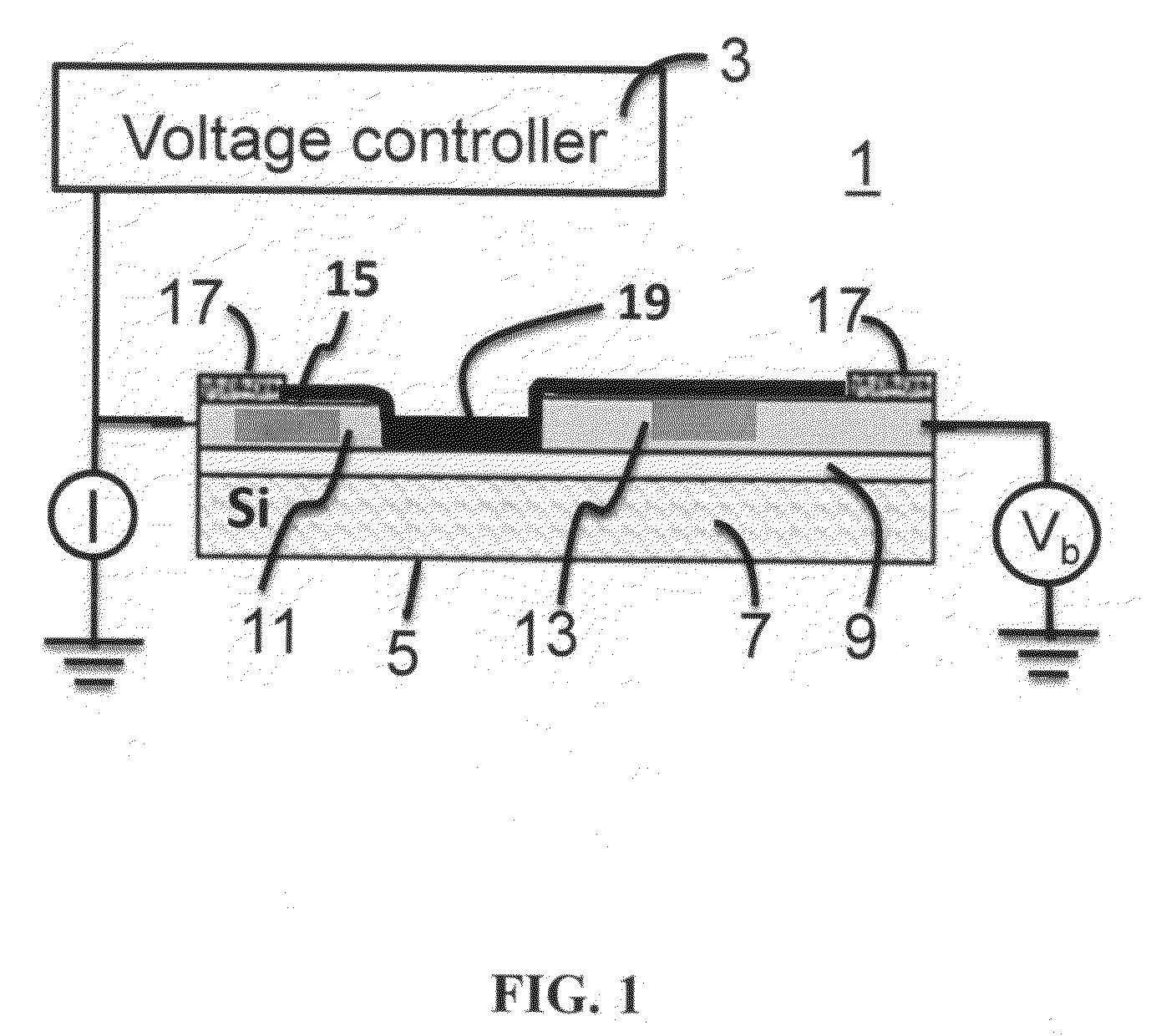
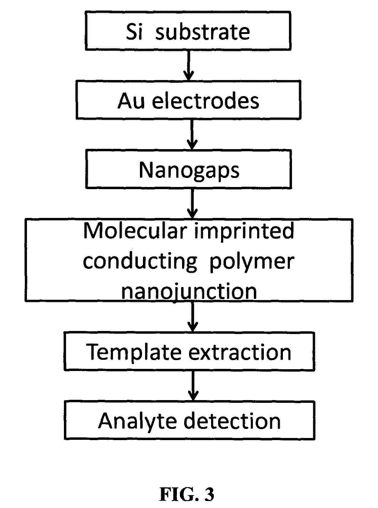
[0090]Volatile organic compound o-xylene was imprinted and detected with molecular imprinted nanosensor. A gold nanogap was first achieved by electrochemically depositing gold materials onto the gold pair of electrodes separated by a 1 μm gap. This nanogap was then bridged with polyaniline copolymer by cycling electrode potential in a solution containing 24 mM regular aniline, 24 mM self-doped aniline (3-aminobenzoic acid), 0.5M sulfuric acid as supporting electrolyte and 800 ppm o-xylene as the target analyte molecule. After formation of the molecular imprinted nanosensor, the analyte molecules were then extracted by cycling the electrode in an analyte free sulfuric acid (0.1M) and detection solution. During the cycling, the solution was replaced for 3-6 times until the current of the nanosensor was stabilized.

[0091]O-xylene was then detected in pH 6.5 solution. Upon exposure to 32 ppb o-xylene, a distinct decrease occurred in the peak current of the sensor. With the concentration ...

example 2

[0092]Detection of a chemical nerve agent simulant, DMMP (Dimethyl methylphosphonate) was demonstrated with DMMP-imprinted nanosensor (solid squares in FIG. 5). The experimental conditions are the same as in EXAMPLE 1, except the template molecules are DMMP in this case. In order to prove that molecular imprinted nanosensor does provide specific binding sites of the analytes, the response of non-imprinted nanosensor to DMMP is also shown in FIG. 5 (solid triangulars). Compared to DMMP-imprinted nanosensor, non-imprinted nanosensor has almost no response to DMMP. Further, DMMP-imprinted nanosensor is sensitive to DMMP, but has no response to PMP (Pinacolyl methyl phosphonate), even the two molecules are very similar on molecular structures, which indicates the great selectivity of our molecular imprinted nanosensor. This work demonstrated that molecular imprinted nanosensor is capable for the detection of toxic organic phosphate chemical nerve agents.


PUM

PropertyMeasurementUnit
areaaaaaaaaaaa
sizeaaaaaaaaaa
sizeaaaaaaaaaa

Abstract

A molecular recognition sensor system is provided incorporating a molecular imprinted nanosensor device formed by the process steps of:(a) fabricating using photolithography a pair of metallic electrodes separated by a microscale gap onto a first electrical insulation layer formed on a substrate;(b) applying a second electrical insulation layer on most of a top surface of said pairs of electrodes;(c) depositing additional metallic electrode material onto said electrode pairs using electrochemical deposition, thereby decreasing said microgap to a nano sized gap between said electrode pairs;(d) electrochemically polymerizing in said nanogap conductive monomers containing a target analyte, thereby forming a conducting polymer nanojunction in the gap between electrode pairs; and(e) immersing resultant sensor device in a solution which removes away the target analyte, and intermittently applying a voltage to the conducting polymer while it is immersed in said solution, thereby swelling and shrinking the conducting polymer to effect a more efficient extraction of target analyte from the conducting polymer.

Description

STATEMENT OF GOVERNMENT INTEREST[0001]This invention was in part made with U.S. government support under contract No. W31P4Q-08-C-0401 awarded by DARPA. Accordingly, the government has certain rights in the invention.BACKGROUND OF THE INVENTION[0002]1. Field of the Invention[0003]The present invention relates in general to a molecular recognition sensor system and process of making same which can be used for the detection of different chemicals in both the liquid and gaseous states and, more particularly, to a sensor device based on a molecular imprinted conducting polymer in nanoscale and process of making same.[0004]2. Description of Related Art[0005]Numerous methods and devices exist for the chemical detection of analytes. For example, prior art methods have attempted to detect analytes by imprinting analyte molecules into a polymer. These methods employ arranging polymerizable monomers around a template followed by polymerization and template removal. The result is a polymer hav...

Claims


Application Information

Patent Timeline
Patent Type & Authority Patents(United States)
IPC IPC(8): C23C28/00
CPCC25D13/04G01N27/128G01N27/327
Inventor LI, XIULANSHASHIDHAR, RANGANATHANMA, YUFENG
Owner POLESTAR TECH
Why Eureka
Try Eureka