Method for producing gallium nitride layer and seed crystal substrate used in same

a gallium nitride and seed crystal substrate technology, applied in the direction of polycrystalline material growth, crystal growth process, transportation and packaging, etc., can solve the problems of low productivity, difficult process control, and single crystal thick layer crack generation, and achieve low dislocation density, good crystal quality, and reproducibility. high

Inactive Publication Date: 2014-08-05
NGK INSULATORS LTD
View PDF16 Cites 7 Cited by
  • Summary
  • Abstract
  • Description
  • Claims
  • Application Information

AI Technical Summary

Benefits of technology

[0012]An object of the present invention is, in growing GaN layer on a seed crystal substrate by flux method, to facilitate spontaneous peeling of the thus grown GaN layer without cracks, to grow the GaN layer over a large area as possible with a high reproducibility and to provide the GaN layer having a low dislocation density and good crystal quality.
[0018]According to the present invention, the grown GaN layer can be spontaneously peeled off without cracks, the GaN layer can be grown over a wide area of the seed crystal layer with a high reproducibility, and the GaN layer having a low dislocation density and good crystal quality can be obtained.

Problems solved by technology

In the case that, however, the gallium nitride (GaN) seed crystal layer is grown on the substrate by vapor phase process by MOCVD and the gallium nitride single crystal is grown thereon by flux method, cracks are generated in the thus grown single crystal thick layer due to the difference of thermal expansion.
According to this process, however, complicated process steps are required, resulting in low productivity.
Further, it is required to terminate the process of forming recesses in the nitride layer before the completion and the process control is difficult.
Since the sapphire-exposed part is present, however, the reproducibility is low when the gallium nitride single crystal is grown by liquid phase epitaxy by the flux method.
According to the method, however, the reproducibility of the peeling of the grown gallium nitride single crystal is low and cracks tend to be generated if successfully peeled.
Further, the single crystal includes periodically generated regions where dislocations are concentrated, so that it cannot be used over the whole surface.
According to this method, however, the reproducibility of the peeling of the thus grown gallium nitride single crystal is low and cracks tends to be generated if peeled.
Further, the single crystal includes periodically generated regions where dislocations are concentrated, so that it cannot be used over the whole surface.

Method used


Image

  • Method for producing gallium nitride layer and seed crystal substrate used in same
  • Method for producing gallium nitride layer and seed crystal substrate used in same
  • Method for producing gallium nitride layer and seed crystal substrate used in same

Examples


example 1

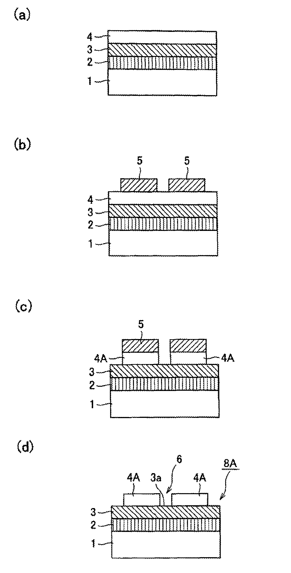
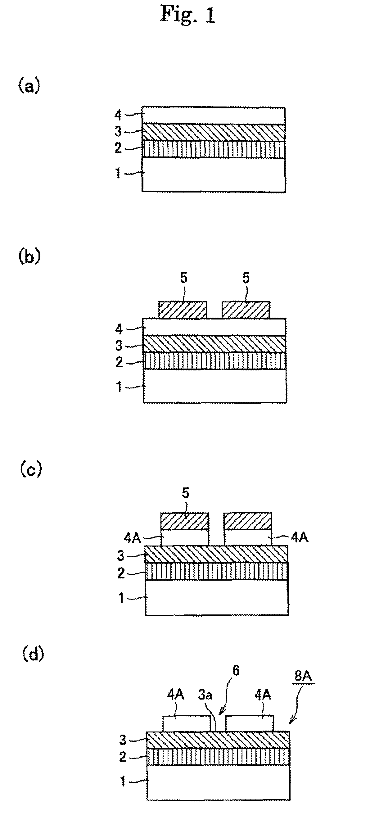
[0072]Gallium nitride single crystal was grown according to the method described referring to FIGS. 1 and 2.

[0073]Specifically, on a surface of a c-face sapphire body 1 having a diameter of 3 inches, an AlN low temperature buffer layer 2, an intermediate layer 3 composed of AlN single crystal and a seed crystal layer 4 composed of gallium nitride single crystal were epitaxially grown by MOCVD method. Raw materials and growth temperature were shown below.

(AlN Low Temperature Buffer Layer 2)

[0074]Raw materials: trimethyl ammonium, ammonia

[0075]Growth temperature: 500° C.

(Intermediate Layer 3 Made of AlN Single Crystal)

[0076]Raw materials: trimethyl ammonium, ammonia,

[0077]Growth temperature: 1200° C.

(Seed Crystal Layer 4 Made of Gallium Nitride Single Crystal)

[0078]Raw materials: trimethyl gallium, ammonia

[0079]Growth temperature: 1050° C.

[0080]In a central region of φ54 mm of the multi-layered template, a mask layer 5 of SiO2 having a shape of stripes each having a width of 0.05 mm a...

example 2

[0083]The gallium nitride crystal plate was produced according to the method described referring to FIGS. 3 and 4. It was carried out according to the same procedure as the Example 1, except that a GaN low temperature buffer layer 2, gallium nitride single crystal layer 9, an intermediate layer 3 made of AlN single crystal and a seed crystal layer 4 made of gallium nitride single crystal were epitaxially grown by MOCVD method on a surface of a c-face sapphire body with a diameter of 3 inches.

(GaN Low Temperature Buffer Layer 2)

[0084]Raw materials: trimethyl gallium, ammonia

[0085]Growth temperature: 550° C.

(Gallium Nitride Single Crystal Layer 9)

[0086]Raw materials: trimethyl gallium, ammonia

[0087]Growth temperature: 1050° C.

(Intermediate Layer 3 Made of AlN Single Crystal)

[0088]Raw materials: trimethyl aluminum, ammonia

[0089]Growth temperature: 1200° C.

(Seed Crystal Layer 4 Made of Gallium Nitride Single Crystal)

[0090]Raw materials: trimethyl gallium, ammonia

[0091]Growth temperature...

example 3

[0093]The seed crystal substrate 8C was produced according to the procedure described referring to FIG. 5.

[0094]Specifically, the GaN low temperature buffer layer 2 and the seed crystal layer 4 composed of gallium nitride single crystal were epitaxially grown on a surface of the c-face sapphire body 1 with a diameter of 3 inches by MOCVD method.

(GaN Low Temperature Buffer Layer 2)

[0095]Raw materials: trimethyl gallium, ammonia

[0096]Growth temperature: 550° C.

(Seed Crystal Layer 4 Made of Gallium Nitride Single Crystal)

[0097]Raw materials: trimethyl gallium, ammonia

[0098]Growth temperature: 1050° C.

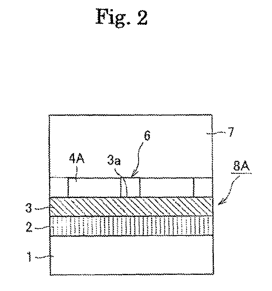
[0099]In a central region of φ54 mm of the GaN template, a mask layer 5 of SiO2 having a shape of stripes each having a width of 0.05 mm and a period of 0.55 mm using photolithography. At this time, the direction of the stripe was made parallel with the direction of m-axis of the gallium nitride single crystal layer 4. The seed crystal layer was etched by using ICP-RIE system and gas mixtu...


PUM

PropertyMeasurementUnit
thicknessaaaaaaaaaa
thicknessaaaaaaaaaa
thicknessaaaaaaaaaa

Abstract

A gallium nitride layer is produced using a seed crystal substrate by flux method. The seed crystal substrate 8A includes a supporting body 1, a plurality of seed crystal layers 4A each comprising gallium nitride single crystal and separated from one another, a low temperature buffer layer 2 provided between the seed crystal layers 4A and the supporting body and made of a nitride of a group III metal element, and an exposed layer 3 exposed to spaces between the adjacent seed crystal layers 4A and made of aluminum nitride single crystal or aluminum gallium nitride single crystal. The gallium nitride layer is grown on the seed crystal layers by flux method.

Description

TECHNICAL FIELD OF THE INVENTION[0001]The present invention relates to a method for growing gallium nitride layers and seed crystal substrates used in the same.BACKGROUND ARTS[0002]Gallium nitride (GaN) thin film crystal draws attention as excellent blue light-emitting devices, has been used as a material for light-emitting diodes and expected as a blue-violet semiconductor laser device for an optical pickup. Recently, it draws attention as a semiconductor layer constituting electronic devices, such as high-speed IC chips, used for mobile phones or the like.[0003]It is reported a method of obtaining a template substrate by depositing a seed crystal layer, such as GaN or AlN, on a single crystal substrate such as sapphire and of growing gallium nitride single crystal on the template substrate.[0004]In the case that, however, the gallium nitride (GaN) seed crystal layer is grown on the substrate by vapor phase process by MOCVD and the gallium nitride single crystal is grown thereon by...

Claims


Application Information

Patent Timeline
Patent Type & Authority Patents(United States)
IPC IPC(8): C30B21/02
CPCC30B19/12C30B9/12C30B19/02H01L31/1856C30B29/406Y10T428/24802
Inventor IMAI, KATSUHIROIWAI, MAKOTASHIMODAIRA, TAKANAOSAKAI, MASAHIROHIGASHIHARA, SHUHEIHIRAO, TAKAYUKI
Owner NGK INSULATORS LTD
Why Eureka
Try Eureka