Microstructured electrode structures

a microstructured electrode and structure technology, applied in the field of structures, can solve the problems of crack formation, pulverisation of anodes, disintegration and exfoliation of existing electronic current collectors, etc., and achieve the effects of reducing transport distances, minimizing or reducing transport distances, and reducing energy storag

Active Publication Date: 2014-09-23
ENOVIX CORP
View PDF31 Cites 24 Cited by
  • Summary
  • Abstract
  • Description
  • Claims
  • Application Information

AI Technical Summary

Benefits of technology

[0015]Among the various aspects of the present invention is the provision of three-dimensional structures for use in energy storage devices such as batteries, fuel cells, and electrochemical capacitors. Such three dimensional structures comprise a layer of microstructured anodically active material on a lateral surface of a backbone structure, the layer containing a void fraction that accommodates significant volume changes in the anodically active material as it cycles between a charged and a discharged state. Advantageously, such three-dimensional structures may be incorporated into two or more battery cells that have been stacked vertically whereby, the shortest distance between the anodically active material and the cathode material in a battery cell is measured in a direction that is orthogonal to the direction of stacking of the battery cells (e.g., in X-Y-Z coordinates, if the direction of stacking is in the Z-direction, the shortest distance between the anodically active material and the cathode material is measured in the X- or Y-direction). Such three-dimensional energy storage devices may produce higher energy storage and retrieval per unit geometrical area than conventional devices. They may also provide a higher rate of energy retrieval than two-dimensional energy storage devices for a specific amount of energy stored, such as by minimizing or reducing transport distances for electron and ion transfer between an anode and a cathode. These devices may be more suitable for miniaturization and for applications where a geometrical area available for a device is limited and / or where energy density requirement is higher than what may be achieved with a laminar device.

Problems solved by technology

Some of these new high capacity materials, such as silicon, aluminum, or tin anodes in lithium batteries have significant volume expansion that causes disintegration and exfoliation from its existing electronic current collector during lithium insertion and extraction.
The formation of lithium silicides when lithium is inserted into the anode results in a significant volume change which can lead to crack formation and pulverisation of the anode.
In such arrangements, one of the significant technical challenges is the ability to collect and carry current from the monolithic electrode to the outside of the battery while efficiently utilizing the space available inside the battery.

Method used


Image

  • Microstructured electrode structures
  • Microstructured electrode structures
  • Microstructured electrode structures

Examples


example 1

[0102]A silicon on insulator (SOI) wafer with a layer thickness of 100 μm / 1 μm / 675 μm (device layer / insulating layer / backing layer) was used as the sample. A hard mask layer of 2000 Å silicon dioxide was sputter deposited on top of the device silicon layer. This wafer was then spin coated with 5 μm of resist and patterned with a mask to obtain a honeycomb shaped structure with the honeycomb wall thickness of 100 μm and the gap thickness of 200 μm. The photoresist was then used as a photomask to remove the silicon dioxide by ion milling.

[0103]The combination of silicon dioxide and photoresist was used as a mask for silicon removal using Deep Reactive Ion Etching (DRIE) in a fluoride plasma. The DRIE was performed until the silicon constituting the device layer in the honeycomb gaps was completely removed, stopping on the oxide layer. The overetch time used was 10% of the total DRIE time in order to remove islands of silicon in the trench floor. Any top photoresist was removed by stri...

example 2

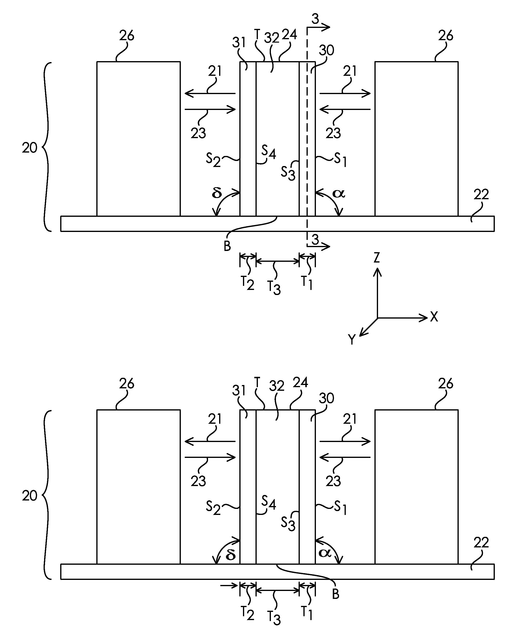
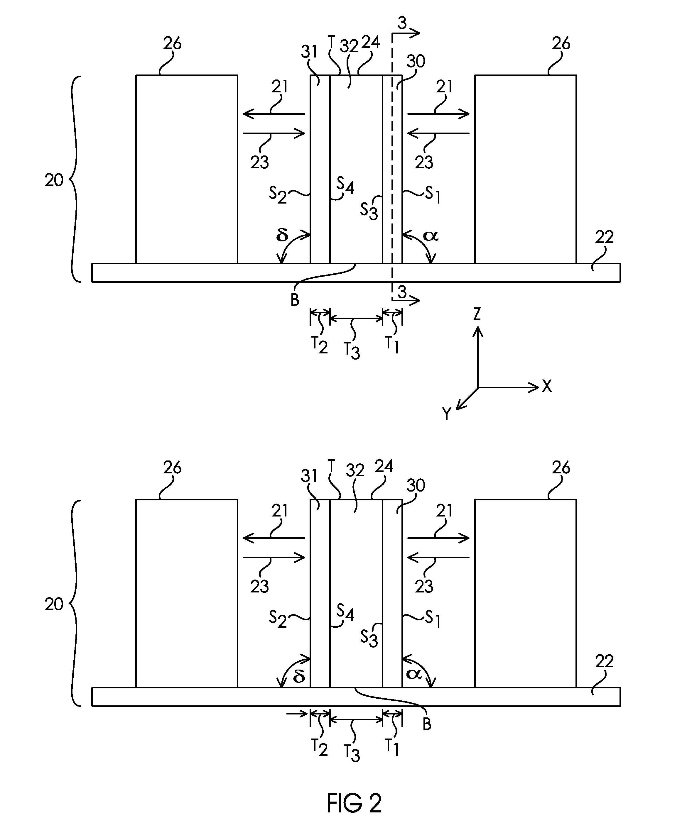
[0107]A silicon on insulator (SOI) wafer with a layer thickness of 100 μm / 1 μm / 675 μm (device layer / insulating layer / backing layer) was used as the sample. 1000 Å of Pd was sputter deposited on top of the device layer followed by a hard mask layer of 2000 Å silicon dioxide. This wafer was then spin coated with 5 μm of resist and patterned with a mask to obtain a comb shaped structure with two interdigitated combs isolated from each other as shown in FIG. 3. The two interdigitated combs also have a landing pad on each side that may be isolated and serve as the contact pad for processing and for the final battery. The photoresist was then used as a photomask to remove the silicon dioxide and palladium by ion milling.

[0108]The combination of silicon dioxide, photoresist, and Pd was used as a mask for silicon removal using Deep Reactive Ion Etching (DRIE) in a fluoride plasma. The DRIE was performed until the silicon constituting the device layer in the mask gaps was completely removed,...

example 3

[0113]A silicon on insulator (SOI) wafer with a layer thickness of 100 μm / 1 μm / 675 μm (device layer / insulating layer / backing layer) was used as the sample. 1000 Å of Pd was sputter deposited on top of the device layer followed by a hard mask layer of 2000 Å silicon dioxide. This wafer was then spin coated with 5 μm of resist and patterned with a mask to obtain a comb shaped structure with two interdigitated combs isolated from each other as shown in FIG. 3. The two interdigitated combs also have a landing pad on each side that may be isolated and serve as the contact pad for processing and for the final battery. The photoresist was then used as a photomask to remove the silicon dioxide and Palladium by Ion Milling.

[0114]The combination of silicon dioxide, photoresist, and Pd was used as a mask for silicon removal using Deep Reactive Ion Etching (DRIE) in a fluoride plasma. The DRIE was performed until the silicon constituting the device layer in the mask gaps was completely removed,...


PUM

PropertyMeasurementUnit
thicknessaaaaaaaaaa
heightaaaaaaaaaa
thicknessaaaaaaaaaa

Abstract

A structure for use in an energy storage device, the structure comprising a backbone system extending generally perpendicularly from a reference plane, and a population of microstructured anodically active material layers supported by the lateral surfaces of the backbones, each of the microstructured anodically active material layers having a void volume fraction of at least 0.1 and a thickness of at least 1 micrometer.

Description

FIELD OF THE INVENTION[0001]The present invention generally relates to structures for use in energy storage devices, to energy storage devices incorporating such structures, and to methods for producing such structures and energy devices.BACKGROUND OF THE INVENTION[0002]Rocking chair or insertion secondary batteries are a type of energy storage device in which carrier ions, such as lithium, sodium or potassium ions, move between an anode electrode and a cathode electrode through an electrolyte. The secondary battery may comprise a single battery cell, or two more battery cells that have been electrically coupled to form the battery, with each battery cell comprising an anode electrode, a cathode electrode, and an electrolyte.[0003]In rocking chair battery cells, both the anode and cathode comprise materials into which a carrier ion inserts and extracts. As a cell is discharged, carrier ions are extracted from the anode and inserted into the cathode. As a cell is charged, the reverse...

Claims


Application Information

Patent Timeline
Patent Type & Authority Patents(United States)
IPC IPC(8): H01M4/80H01M4/134
CPCH01M4/80H01M4/134B82Y30/00H01G4/008H01G4/012H01G4/015H01G4/32H01M4/1395H01M4/386H01M4/70H01M10/0436H01M10/052H01M10/0525H01M10/054H01M10/0564H01M2004/021H01M2220/30H01M2300/0017Y02E60/122H01M4/38Y02E60/10Y02P70/50H01M2004/027
Inventor LAHIRI, ASHOKSPOTNITZ, ROBERTSHAH, NIRAVRAMASUBRAMANIAN, MURALIRUST, III, HARROLD J.WILCOX, JAMES D.ARMSTRONG, MICHAEL J.BRUSCA, BRIAN E.CASTLEDINE, CHRISTOPHER G.LAUCHLAN, LAURIE J.
Owner ENOVIX CORP
Why Eureka
Try Eureka