High speed low loss gate drive circuit

a gate drive circuit and low loss technology, applied in the field of electronic gate drive circuits, can solve the problems of gate drive circuits further suffering from loss of gate charge, gate driver power loss, and disadvantageous limitation of the turn-on and turn-off speed of some types of semiconductor switches such as mosfet switches and igbt switches, so as to maximize dv/dt immunity, reduce the loss of turn-off switching, and high frequency operation

Active Publication Date: 2014-09-30
GENERAL ELECTRIC CO
View PDF17 Cites 17 Cited by
  • Summary
  • Abstract
  • Description
  • Claims
  • Application Information

AI Technical Summary

Benefits of technology

[0016]The embodiments of the present invention described herein provide a systematic approach for driving a power semiconductor switching device of a high frequency converter in a new and improved high speed low loss gate driver circuit. The new gate driver circuit comprises a full bridge configuration with an inductor connected between the mid points of the bridge. Two capacitors, Cpos and Cneg, connected in series, are coupled into the DC link of the bridge with a gate DC power supply Vc as an input. The low voltage switches are controlled in way that the gate driver circuit provides a programmable magnitude of the discharge current to turn the power switch device off fast enough to reduce turn-off switching loss and keep voltage overshoot in a safe limit A negative voltage bias is applied to the gate to maximize the dv / dt immunity for the power MOSFET when it is in an off state. The gate driver circuit provides a tunable turn-on current to match switching characteristics of other power devices used in a practical application. Furthermore, the gate driver circuit recovers turn-on / off gate energies stored in the input capacitance of the power switch to ensure a high frequency operation.

Problems solved by technology

Turn-on and turn-off speeds of some types of semiconductor switches such as MOSFET switches and IGBT switches are disadvantageously limited by R-C circuit elements when employed in conventional voltage source gate drive circuits.
Such voltage source gate drive circuits further suffer from lost gate charge.
Although the conventional gate driver ICs are easy to use, they usually suffer from two major issues.
One issue is related to the gate driver power losses and the other is related to the operation modes of the power switch they drive.
The gate driver loss becomes a limiting factor when the operation frequency enters MHz region.
They, however, lack a systematic approach to deal with the issues associated with the power switch operation modes where the effects of parasitic components as well as transient and extreme operating conditions are important.
It is intuitively obvious that switching losses exist due to high current and high voltage being present in the power device simultaneously for a short period corresponding to the Miller plateau interval when the drain voltage goes through its switching transient and linear interval when the drain current changes responding to the change in the gate voltage.
The drain inductance LD on the other hand acts as a beneficial turn-on snubber but produces an overshoot in the drain-to-source and an increase in turn-off switching losses.
In the hard switching case the turn-on speed is usually limited by the turn-off, or reverse recovery speed of the diode, and not by the strength of the gate drive circuit.

Method used


Image

  • High speed low loss gate drive circuit
  • High speed low loss gate drive circuit
  • High speed low loss gate drive circuit

Examples


first embodiment

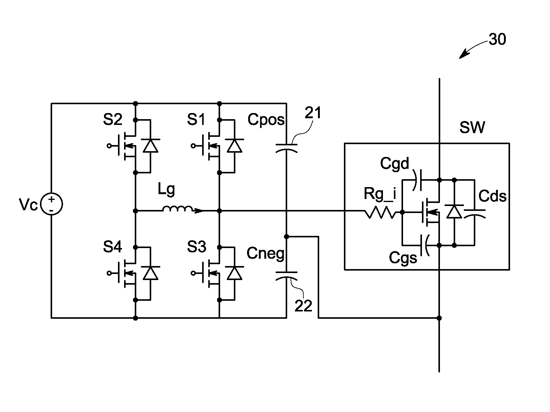
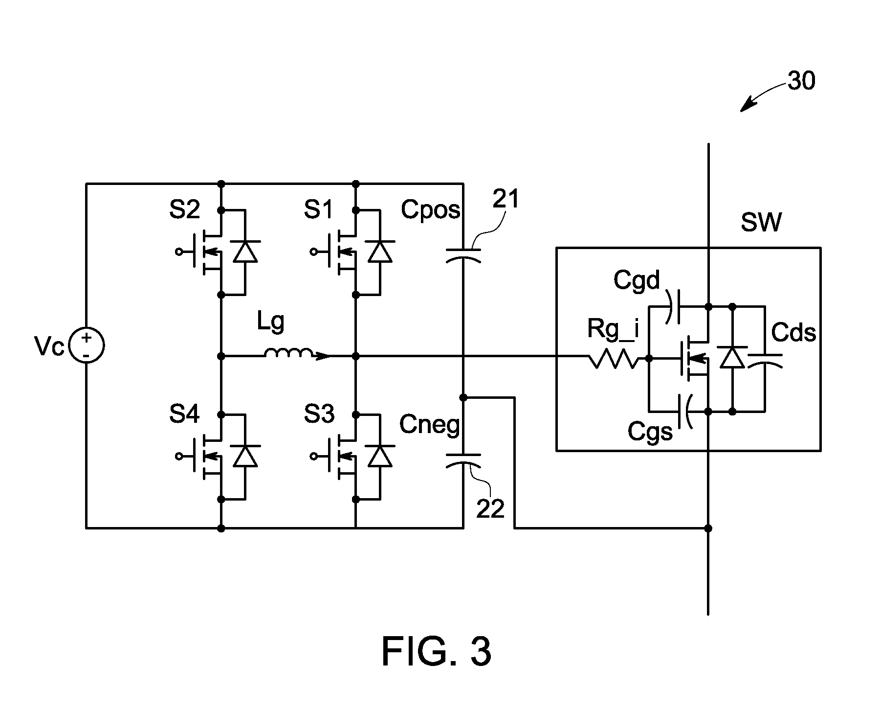
[0029]FIG. 3 is a circuit diagram of a gate driver circuit 30 according to a preferred first embodiment of the present invention. As shown in FIG. 3, two capacitors 21, 22 are connected in series forming a voltage divider. The voltage divider ratio could be simply determined by a high resistive resistor divider connected in parallel with the capacitor pair. These two capacitors 21, 22 preferably have a low ESR (equivalent series resistance) and a low ESL (equivalent series inductance) with a compact size, such as SM (surface mount) ceramic capacitors. The SM capacitor Cneg 22 and the low voltage MOSFET S3 are arranged closely, both physically and electrically, so that a loop area that is as small as possible is formed with the gate input capacitance of the power switch, to maximize the dv / dt immunity. The loop area formed by MOSFET S4, Lg, gate input capacitance and Cneg is less important in the electromagnetic susceptibility point of view, but it is favorable to make it small so th...

embodiment 100

[0034]FIG. 10 illustrates another gate drive circuit embodiment 100, where a negative voltage is generated with Cneg 102 and a zener+diode branch 104.


PUM


Abstract

A gate drive circuit includes an insulated gate semiconductor switch. A controlled current source is connected to the semiconductor switch gate terminal to provide a gate drive circuit that is responsive to recycled gate charge corresponding to an internal gate capacitance of the insulated gate semiconductor switch.

Description

[0001]This invention was made with Government support under contract number DE-FC26-08NT05868, awarded by the U.S. Department of Energy. The Government has certain rights in the invention.BACKGROUND[0002]The subject matter of this disclosure relates generally to electronic gate drive circuits and more particularly to a system and method for providing a high speed, low loss gate drive circuit for semiconductor switches such as, without limitation, metal oxide semiconductor field effect transistor (MOSFET) switches, insulated gate bipolar transistor (IGBT) switches, and thyristor switches.[0003]Turn-on and turn-off speeds of some types of semiconductor switches such as MOSFET switches and IGBT switches are disadvantageously limited by R-C circuit elements when employed in conventional voltage source gate drive circuits. Such voltage source gate drive circuits further suffer from lost gate charge.[0004]As shown in FIG. 1, a conventional gate driver circuit 10 is typically implemented i...

Claims


Application Information

Patent Timeline
Patent Type & Authority Patents(United States)
IPC IPC(8): H03K3/00
CPCH03K17/04123H03K17/163H03K2217/009
Inventor TAO, FENGFENGSADDOUGHI, SEYED GHOLAMALIHERBON, JOHN THOMAS
Owner GENERAL ELECTRIC CO
Why Eureka
Try Eureka