High efficiency quantum well waveguide solar cells and methods for constructing the same

a solar cell and quantum well technology, applied in the field of semiconductor-based photovoltaic energy converters, can solve the problems of limited device operation voltage, affecting the generation of current, and reducing the operation voltage of conventional quantum structured solar cells, so as to minimize the underlying diode dark current, increase the optical path length, and enhance the open circuit voltage of quantum well waveguide solar cell structures

Active Publication Date: 2014-12-30
MAGNOLIA SOLAR
View PDF2 Cites 17 Cited by
  • Summary
  • Abstract
  • Description
  • Claims
  • Application Information

AI Technical Summary

Benefits of technology

[0007]This invention overcomes the disadvantages of the prior art by providing a solar cell design and process for constructing a solar cell that employs an extended region of wide energy gap material within the depletion region adjacent to the emitter and incorporating step-graded quantum wells. This structure enhances the open circuit voltage of quantum well waveguide solar cell structures. Advanced quantum well solar cell structures both minimize the underlying diode dark currents and increase the optical path length to deliver solar electric conversion efficiencies exceeding 30% over a wide range of spectral conditions.
[0008]In an illustrative embodiment, a conventional homojunction structure incorporates an InGaAs well embedded within a GaAs matrix. To reduce the diode dark current, wider energy-gap InGaP and AlGaAs material is employed in the emitter and inserted into the depletion region adjacent to the emitter, forming an extended wide band gap emitter heterojunction structure. Illustratively, the refractive index contrast is further enhanced by employing an AlGaAs base layer.

Problems solved by technology

The operational voltage of the device is limited by the dark current characteristics of the underlying PN or PIN junction, among other limiting characteristics.
However, photon absorption, and thus current generation, is hindered in conventional quantum structured solar cells by the limited path length of incident light passing vertically through the device.
Moreover, the insertion of narrow energy-gap material into the device structure often results in lower voltage operation, and hence lower photovoltaic power conversion efficiency.
Coupling of normally incident light into lateral optical propagation paths has been reported to lead to increases in the short circuit current of InP / InGaAs quantum well waveguide solar cells coated with nanoparticles.
However, maintaining high open circuit voltage remains a universal challenge for all quantum well and quantum dot solar cell devices.

Method used


Image

  • High efficiency quantum well waveguide solar cells and methods for constructing the same
  • High efficiency quantum well waveguide solar cells and methods for constructing the same
  • High efficiency quantum well waveguide solar cells and methods for constructing the same

Examples


Embodiment Construction

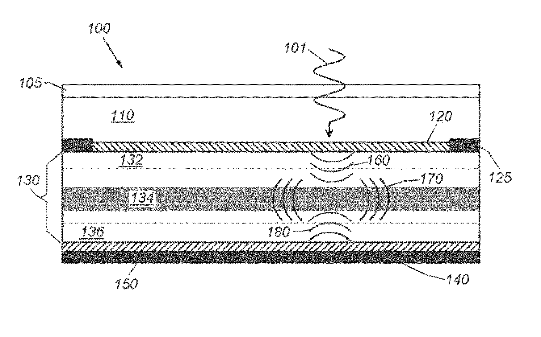
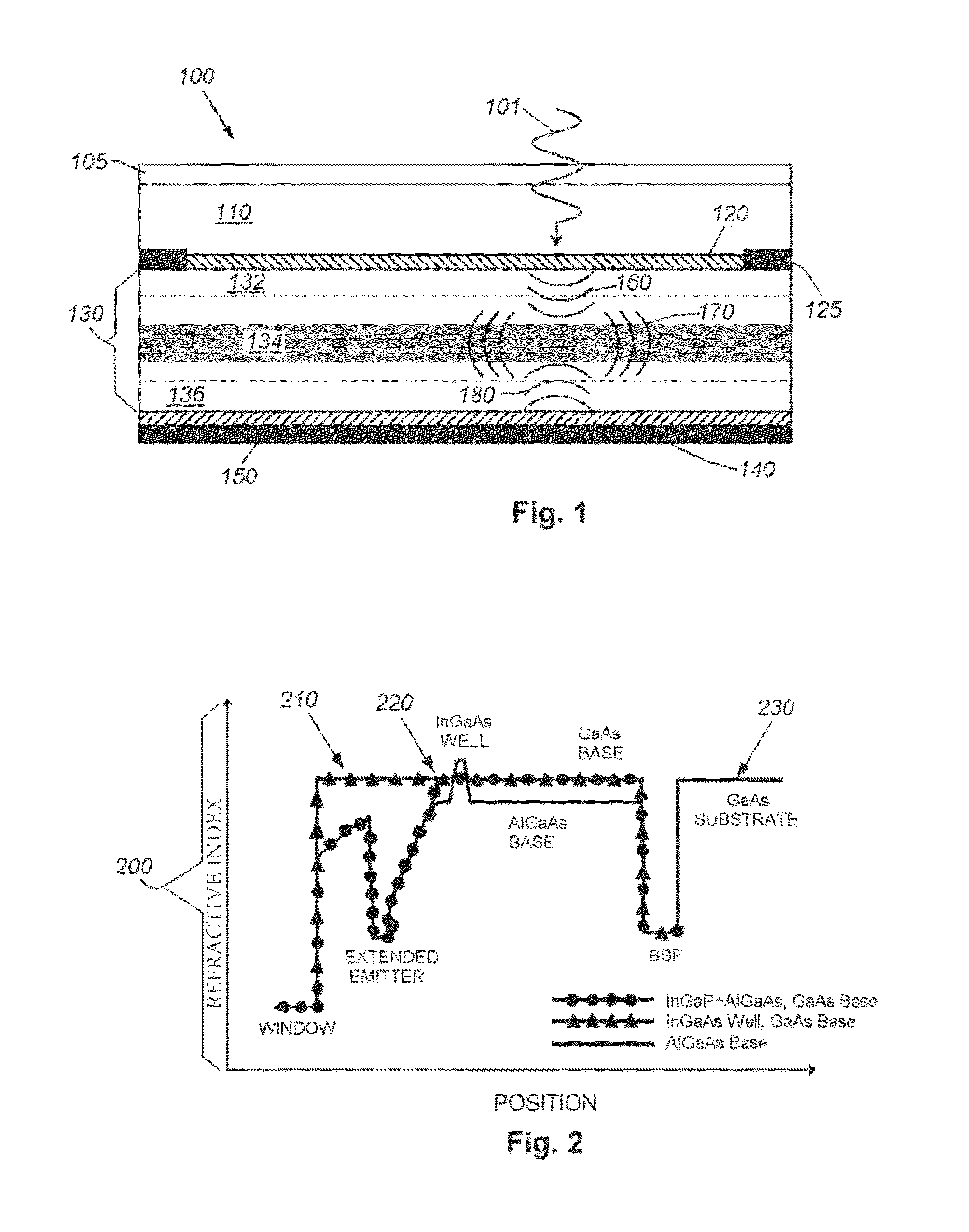
[0020]A typical thin film solar cell structure contains a limited volume of low band gap material, and thus requires advanced light trapping structures to reach its potential performance levels. Light management is achieved by assuring that incident photons are not lost due to reflections but are instead directed into the semiconductor absorbing layers. The scattering of incident light to ensure each photon has a non-normal trajectory is a strategy for increasing the optical path length of photons within the absorption layer. In addition, the application of a back reflector to bounce any unabsorbed photons back up into the active layers of the device is a beneficial aspect of any effective photovoltaic light trapping scheme. However, the most effective light trapping schemes will also direct light horizontally into the plane of the absorbing layer. Waveguide structures in which thin layers of high refractive index material are surrounded by low refractive index material provide a ph...


PUM


Abstract

Photon absorption, and thus current generation, is hindered in conventional thin-film solar cell designs, including quantum well structures, by the limited path length of incident light passing vertically through the device. Optical scattering into lateral waveguide structures provides a physical mechanism to increase photocurrent generation through in-plane light trapping. However, the insertion of wells of high refractive index material with lower energy gap into the device structure often results in lower voltage operation, and hence lower photovoltaic power conversion efficiency. The voltage output of an InGaAs quantum well waveguide photovoltaic device can be increased by employing a III-V material structure with an extended wide band gap emitter heterojunction. Analysis of the light IV characteristics reveals that non-radiative recombination components of the underlying dark diode current have been reduced, exposing the limiting radiative recombination component and providing a pathway for realizing solar-electric conversion efficiency of 30% or more in single junction cells.

Description

RELATED APPLICATIONS[0001]This application claims the benefit of U.S. Provisional Application Ser. No. 61 / 525,707, filed Aug. 19, 2011, entitled HIGH EFFICIENCY QUANTUM WELL WAVEGUIDE SOLAR CELLS AND METHODS FOR CONSTRUCTING THE SAME, the entire disclosure of which is herein incorporated by reference.STATEMENT REGARDING FEDERALLY SPONSORED RESEARCH OR DEVELOPMENT[0002]This invention was made with U.S. government support under Grant Number NNX11CE59P, awarded by the National Aeronautics and Space Administration (NASA) and Grant Number ERDA1-0000021389 awarded by the New York State Energy Research and Development Authority (NYSERDA). The government may have certain rights in this invention.FIELD OF THE INVENTION[0003]This invention relates to semiconductor-based photovoltaic energy converters, also known as “solar cells,” and to the design and fabrication of the same.BACKGROUND OF THE INVENTION[0004]With appropriate electrical loading, photovoltaic solid state semiconductor devices, c...

Claims


Application Information

Patent Timeline
Patent Type & Authority Patents(United States)
IPC IPC(8): H01L31/00
CPCH01L31/00H01L31/035236H01L31/0735H01L31/056Y02E10/52Y02E10/544Y02E10/548Y02P70/50H01L31/03046H01L31/035209H01L31/075H01L31/1844
Inventor WELSER, ROGER E.SOOD, ASHOK K.
Owner MAGNOLIA SOLAR
Why Eureka
Try Eureka