High frequency power combiner/divider

a high-frequency power combiner and divider technology, applied in the direction of amplifiers, waveguides, amplifiers with semiconductor devices/discharge tubes, etc., can solve the problems of high voltage risk, large drawbacks of twt amplifiers, and large size and weight, so as to improve overall sspa and reduce height , the effect of high isolation

Inactive Publication Date: 2015-06-23
CUBIC CORPORATION
View PDF52 Cites 93 Cited by
  • Summary
  • Abstract
  • Description
  • Claims
  • Application Information

AI Technical Summary

Benefits of technology

[0011]In exemplary configurations, power combining structures of the present invention may include an air-coax input power divider; pre-driver, driver, sub-amplifier modules (which may themselves include an air-coax divider and combiner, phase shifters, filters and / or linearizers), a microfabricated output waveguide combiner; and / or, an air-coax or waveguide output. The power amplifier may be made in a modular format allowing building blocks that can be independently tested and which aid in scalable products that reuse similar or identical components in their architecture. In exemplary configurations, the relationships for the mechanical elements which govern the electromagnetic properties may be addressed during the forming process. Likewise, precision integration of these components may allow them to be assembled with the necessary tolerances and precision for an intended application.
[0012]In exemplary configurations, the waveguide combiner portion of the SSPA may be fed by a number of amplifier modules (or “sub-modules”) feeding each input port and the respective input port end launcher of said hollow core waveguide power combiner. Each of these amplifier modules may have multiple MMIC chips (e.g., such as 2 chips, 4 chips or 8 chips using a 2-way or 4-way or 8-way Wilkinson or Gysel sub-combiner). Such combiners as the Wilkinson or Gysel can provide higher isolation than a hollow waveguide combiner alone, for example, and can provide isolation among MMIC chips. This can help provide graceful degradation in the event of any partial or individual chip failures of the overall combining performance. For example, with an 8-way radial hollow waveguide power combiner, 32 or 64 MMIC chips may be combined together when fed by eight 4-way or 8-way micro-coaxial power combining sub-modules. In other configurations, 4-way, 8-way, 10-way, or N-way radial combiners can be used, and additional or fewer MMIC chips may be combined together. Thus the overall SSPA may be improved by combining the port protection and isolation of 2 or more chips combined using a 2 or n-way Wilkinson or Gysel, each of which modules feed an input port of the hollow core waveguide combiner. Thereby the SSPA is benefited by the low loss of hollow core waveguide combining and the port to port isolation of a transmission line combiner.
[0013]In another of its aspects, the present invention may enable precision formation of waveguide devices. For example, the structures of the present invention, such as the combining waveguide structure, may be built using a microfabrication process or another precision manufacturing technique, such as, for example, precision milling, stereolithography, electrochemical forming, chemical or photochemical etching, EDM machining, solid printing, deep RIE, stamping, LIGA, laser solidification or powders or liquids, laser machining, casting, PolyStrata® processing, transfer molding, or injection molding. Depending on the frequency of operation the waveguide combiner can be fabricated as a reduced height waveguide or as a full height waveguide at higher frequency (e.g., about 1 mm at V-band). In FIGS. 1A-15B, the combining waveguide structure may have such a reduced height depending on the frequency. Because of the ability to reduce the waveguide height, the size and weight of the combiner may be significantly minimized at lower frequency where large waveguide are needed. Since power combining may be within either air-coax and / or a waveguide combiner / divider, the SSPA or system overall loss may be lower than other designs. Furthermore, as the manufacturing tolerances may be in the micron range, the phase error may be further reduced so that the efficiency of the SSPA may be significantly improved. Several parameters in the combiner such as the end launcher 100 are very sensitive to fabrication tolerances particularly at extremely high frequency, mm wave and sub-mm wave. Fabrication precision and accuracy in this novel approach can as well keep the low loss combining performance up to such high frequencies (e.g., from 30 GHz to 300 GHz and can be applied up to 1 THz).
[0014]In a further aspect, the present invention may include a electromagnetic end launcher to provide conversion of an RF transmission line mode, such as coax, to / from a hollow waveguide radiation mode, which may have relatively low loss and increased ease of fabrication. Such an electromagnetic end launcher may be integrated directly into the waveguide manufacturing process to prevent alignment and bonding errors, whereas prior designs may have used independently fabricated, aligned, and tuned and bonded E-probes for coax to waveguide transition. (In such E-probe designs, the non-air-coax structure may cause higher loss at high frequencies, such as at the Ka-, V- and W-bands.) Additionally, a coax or air-coax to waveguide end launchers may be microfabricated monolithically with the microfabricated waveguide combiner to provide enhanced manufacturing control and / or enhanced performance. Moreover, alignment features and / or precision mechanical interlocks that enable precision registration and / or connection of such launchers, and / or MMICs, and / or connectors and / or E-probes may be incorporated into the formation process to enable precision integration and assembly of such parts with precision in the tolerances and the electrical, mechanical, thermal, and / or electromagnetic connections between them.
[0015]An added benefit of the electromagnetic end launcher designs that are grounded is the mechanical stability of such structures to vibration and thermal and mechanical shock. Having an end of the electromagnetic end launcher, or a region near an end of the electromagnetic end launcher formed, fused, adhered, or mechanically attached to a hollow waveguide wall region can suppress or prevent vibrations, oscillations, and provides stability for the geometric relations in a highly fixed manner. Eliminating such vibrations of the launcher while it is exposed to vibration or shock can prevent phase noise and other degradation of the amplified signal quality when said SSPA is exposed to such environments which are often encountered in aerospace and mobile terrestrial applications. This is particularly important when the environment for mounting or housing the SSPA is subject to severe vibrations and accelerations as may be found in a moving vehicle such as helicopter, jet, car, tank, or rocket. When formed through a multi-layer microfabrication build process such as PolyStrata®, such metal structures may be formed layer by layer. However, it should be clear as described in the PolyStrata® processes that metal could also be affixed or adhered to a defined region of dielectric such as a dielectric pedestal. The shapes and materials can be optimized using design and optimization software such as HFSS• produced by Ansoft.
[0016]Exemplary configurations of the present invention may include one or multiple sub-modules each of which typically includes multiple MMIC chips. The sub-module may be tested separately before final assembly and / or may be replaced or repaired. All of the MMIC chips in a sub-module may be placed on a common heat sink for improved heat dissipation. Also such sub-module amplifiers may be similarly bonded to regions in or on a common planar thermal heat sink or ground plane. FIG. 15A shows an example of this architecture where modules 1514 or 1614, the waveguide power combiner 800, the input divider 1516 could all be placed onto on a common heatsink. The SSPA 1500 shows an example of such architecture, where the thermal management will be greatly enhance, improving weight, power consumption and longer term reliability to name a few. Removing the heat primarily down and out from one primary plane simplifies the housing and mounting requirements of the SSPA system and allows the areas above and around the plane to be used for interconnects and other components. Such an approach may produce a substantially more compact amplifier design than, for example, a more traditional radial waveguide approach, and may also simplify the supporting structures, such as the thermal management support. Such planar launchers and combiners may help reduce the number of layers and / or height and / or thickness required to produce the assembly.

Problems solved by technology

However, the drawbacks of TWT amplifiers are significant, such as considerable size and weight.
Further, TWT amplifiers require a high voltage driver, such as an electronic power conditioner, that in turn necessitates additional complex accessory circuits and involves high voltage risk.
To work linearly, TWT amplifiers are normally backed off from their saturated output power or additional linearization circuits are added, and linearization circuitry usually results in a dramatic increase in the system complexity and cost.
This inevitable variability can often lead to running an amplifier either at too high or too low of a power level for the conditions at hand and can lead to unnecessarily high levels of power consumption.
Furthermore, often power amplifiers are required to feed systems that demand continuous operation without substantial interruption, and therefore may require a back-up to be ready and waiting in the event of failure of the primary amplifier.
Existing SSPA designs are based on power combiners, such as radial combiners, but they sometimes tend to be bulky, heavy, and / or require complex machining.
Even though split block waveguide structure / combiners can be used to reduce machining complexity, the SSPA may suffer from both leakage problems and joining problems.
For example, to minimize the insertion loss and return loss, integration of conductive signal line based waveguides, such as microstrip, CPW (Co-Planar Waveguide), or coax, with hollow waveguides is additionally complicated due to tolerances and alignment that may be required.
Because a high power SSPA usually has high loop gain, the RF leakage of a multi-part or traditional combiner system could severely degrade the system performance.
In addition, existing SSPA designs may be difficult to manufacture at high frequency, for example at V-band and W-band, and their size and weight may increase the cost of launching a satellite into orbit or make UAV (Unmanned Aerospace Vehicle) applications impossible.
One difficulty faced by previous SSPA designs is that they do not work well at high frequencies.
Commonly used components, such as stripline, microstrip line, coax, splitter and combiner structures, all include parasitic effects and may suffer material / substrate loss.
Parasitic effects of interconnections, splitters, combiner structures, and / or the materials used to propagate the signal may contribute to the frequency limitations inherent with the SSPA designs in the art.
As frequency increases, the tolerances and accuracy between the electromagnetically critical elements within the passive combining and feed structures become increasingly sensitive to error and so methods of construction that work well at several or several 10's of GHz are unsuitable for obtaining high performance at 40, 60, 90, 180, or 240 GHz.
Many individual pieces of existing SSPA designs require complex machining, such as, for example, extremely high precision milling, wire Electric Discharge Machining (EDM) and / or laser processes which lead to relatively high manufacturing costs and challenges in the part integration and bonding to produce a device with sufficiently good electromagnetic properties, for example, in terms of accumulative insertion and / or return loss.
Additionally, in some circumstances, required machining tolerances at high frequencies make mass production difficult because every SSPA may have to be manually assembled and tuned to compensate for the manufacturing tolerances.

Method used


Image

  • High frequency power combiner/divider
  • High frequency power combiner/divider
  • High frequency power combiner/divider

Examples


Embodiment Construction

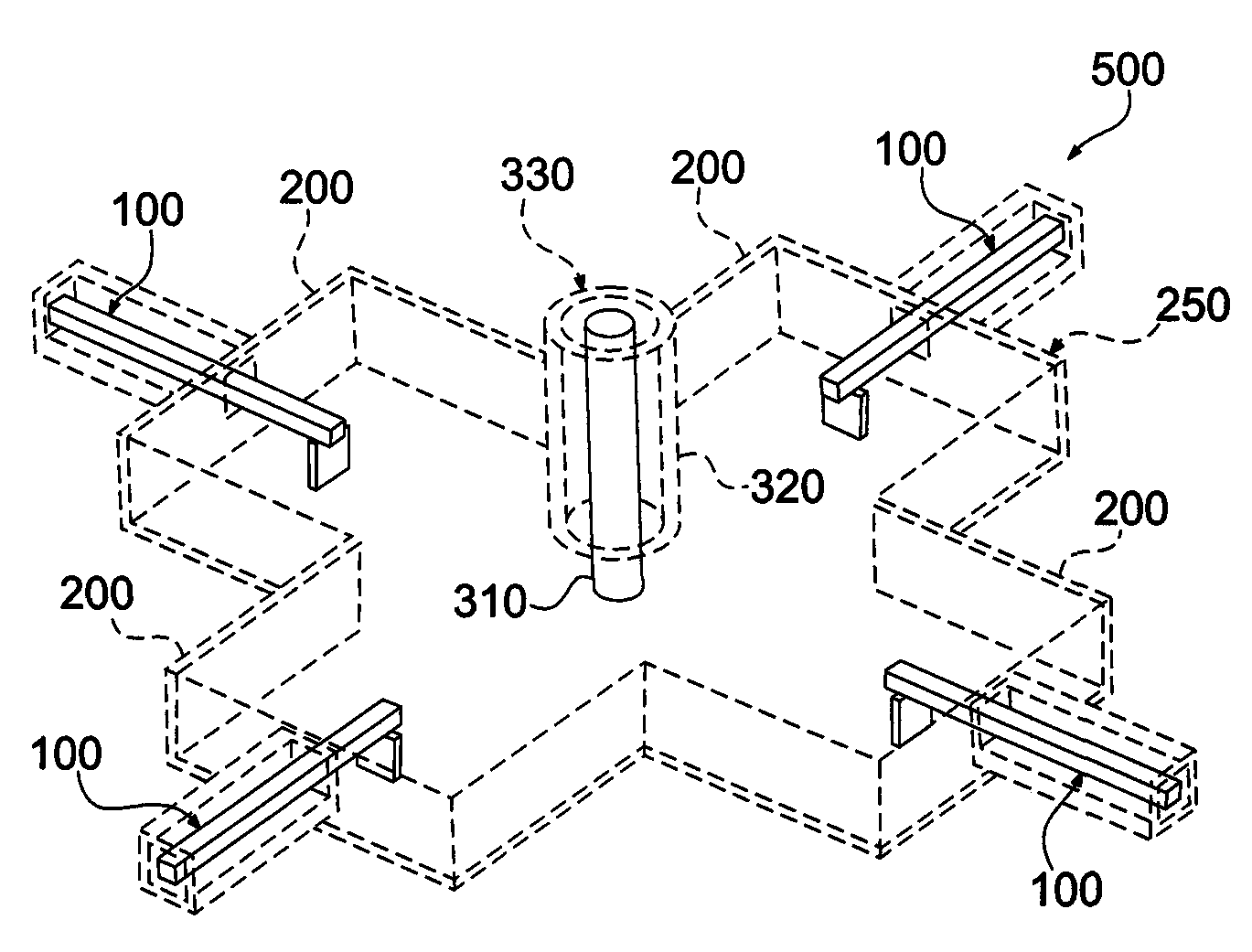
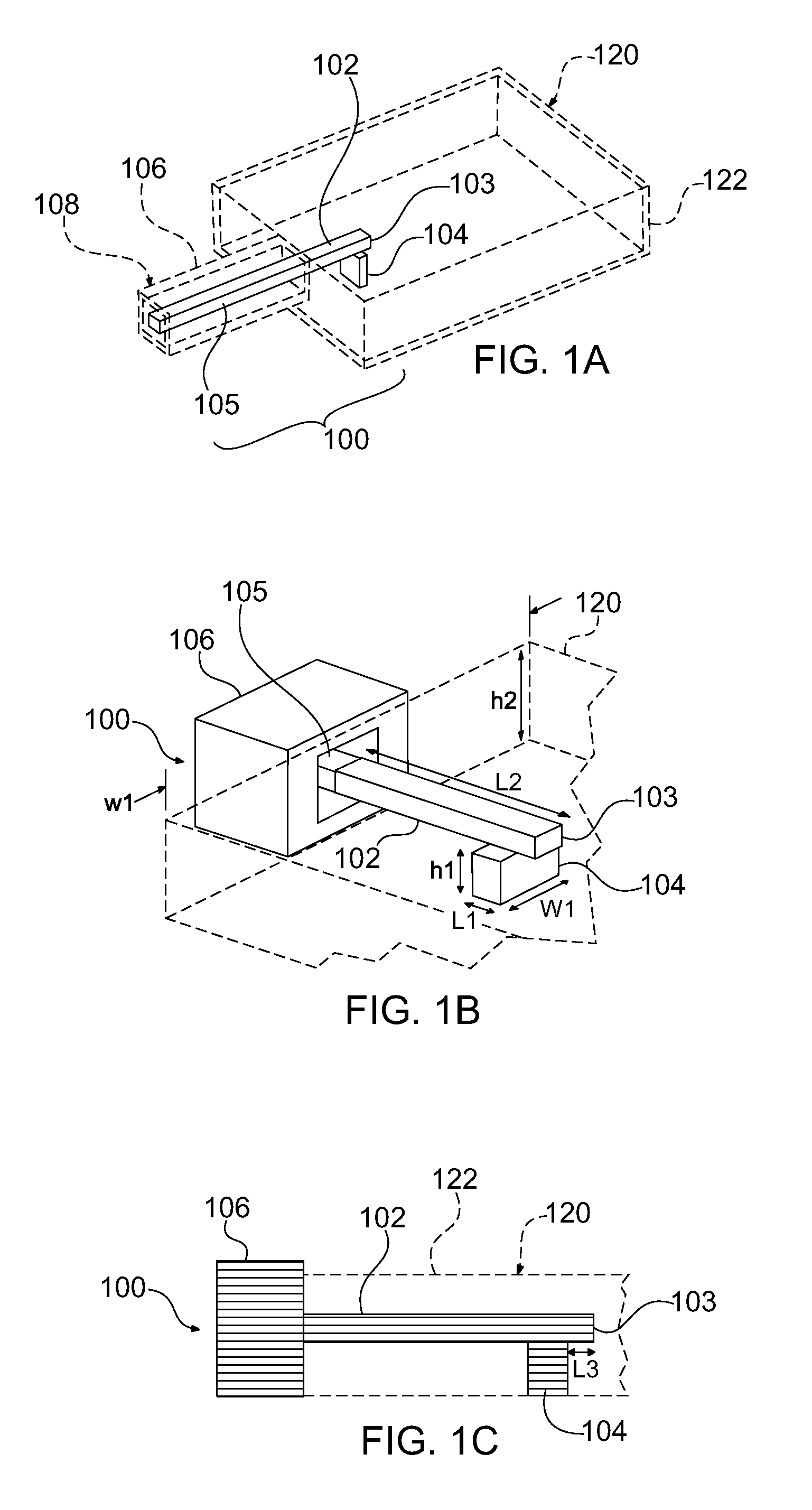
[0040]In view of the aforementioned needs in the art, in one of its aspects the present invention provides waveguide power combiner / dividers which are designed with the recognition that RF power can be more efficiently combined / divided when the power is contained in radiation modes of hollow waveguides rather than in RF signals in transmission lines. (As used throughout this disclosure, the term “combiner / divider” is used to refer to a device having a structure which can either combine or divide RF power, depending on how the device is incorporated in an overall system architecture. For example, if a combiner / divider includes N ports at a first end and a single port at a second end, the combiner / divider may function as a divider if an input signal is provided to the single port and divided output signals delivered to the N ports; conversely, the combiner / divider may function as a combiner if input signals are provided to the N ports and a combined signal is output from the single po...


PUM


Abstract

Radio frequency (RF) power amplifiers are provided which may include high power, wideband, microwave or millimeter-wave solid state power amplifiers based on waveguide power combiner / dividers.

Description

RELATED APPLICATIONS[0001]This application claims the benefit of priority of U.S. Provisional Application No. 61 / 580,100, filed on Dec. 23, 2011, the entire contents of which application is incorporated herein by reference.GOVERNMENT LICENSE RIGHTS[0002]This invention was made with government support under contract number #FA8650-11-C-1159 awarded by U.S. Air Force. The government has certain rights in the invention.FIELD OF THE INVENTION[0003]The present invention relates generally to radio frequency (RF) power amplifiers, and more particularly but not exclusively to high power, wideband, microwave or millimeter-wave solid state power amplifiers based on waveguide power combiner / dividers.BACKGROUND OF THE INVENTION[0004]Current high power microwave amplifier applications usually employ travelling wave tubes (TWT) to provide microwave power magnification. However, the drawbacks of TWT amplifiers are significant, such as considerable size and weight. Further, TWT amplifiers require a...

Claims


Application Information

Patent Timeline
Patent Type & Authority Patents(United States)
IPC IPC(8): H01P5/12H01P3/12H01P11/00H03F3/195H03F3/21
CPCH01P3/12H01P11/002H03F3/195H03F3/211H01P5/024H01P5/12H03F3/602
Inventor WU, DONALD X.SHERRER, DAVID W.ROLLIN, JEAN-MARC
Owner CUBIC CORPORATION
Why Eureka
Try Eureka