Surface acoustic wave monitor for deposition and analysis of ultra-thin films

a surface acoustic wave and monitor technology, applied in the direction of instruments, vacuum evaporation coating, and fluid analysis using ultrasonic/ultrasonic/infrasonic waves, can solve the problems of limiting the widespread adoption of this potentially beneficial technology, high cost of high purity single wall nanotubes (swnts), and affecting the quality of materials. , the effect of low cost, small size and ruggedness

Active Publication Date: 2015-09-01
SENSANNA
View PDF11 Cites 11 Cited by
  • Summary
  • Abstract
  • Description
  • Claims
  • Application Information

AI Technical Summary

Benefits of technology

[0028]A surface acoustic wave (SAW) based thin film deposition monitor device and system for monitoring the deposition of ultra-thin films and nanomaterials and the analysis thereof is characterized by acoustic wave device embodiments that include differential delay line device designs, and which can optionally have integral reference devices fabricated on the same substrate as the sensing device, or on a separate device in thermal contact with the film monitoring / analysis device, in order to provide inherently temperature compensated measurements. These deposition monitor and analysis devices can include inherent temperature compensation, higher sensitivity to surface interactions than quartz crystal microbalance (QCM) devices, and the ability to operate at extreme temperatures. This device structure will operate to provide real-time information on deposition rate and properties of deposited films for continuous, discontinuous, or partially continuous films of as little as several angstroms thickness, providing a platform useful for characterizing a wide range of ultra-thin films, including nanomaterials such as nanocluster metal films, carbon nanotubes, and other nanostructured materials. A transceiver circuit can be configured to provide wired or wireless interrogation of the deposition monitor and analysis device or group of devices.
[0029]Embodiments of the invention comprise novel acoustic wave device embodiments that include differential delay line device designs, and which can optionally have integral reference devices fabricated on the same substrate as the sensing device, or on a separate device in thermal contact with the deposition monitor device, in order to provide inherently temperature compensated measurements. Thus, these devices would be able to operate over a wide range of temperatures without suffering the temperature-induced inaccuracies of current QCM and SAW sensors. Previously described SAW microbalance devices generally use either the resonance frequency of a SAW resonator (measured directly, or as phase, or derived using the Fourier Transform of the amplitude of the sensor impulse response), or the time delay of a SAW delay line as the parameter measured to determine mass loading or sensor response. The deposition monitor device that is the subject of embodiments of the present invention is fundamentally different from any of these approaches in than it utilizes a reflective transversal filter response S11 as an indicator of the device mass loading due to the deposited film, as well as the film conductivity, and film viscoelastic properties. As surface mass, conductivity, and viscoelastic film properties of the deposition monitor device change, the reflective transversal filter response shifts or fundamentally changes its nature in both the frequency and time domains. Measurement of the power spectral density of the sensor response provides a sensitive means of determining the device temperature, and the characteristics of the deposited film. The changes can also be observed in (or extracted from) the time domain response. These devices can be designed to respond to film conductivity, allowing measurement of extremely thin (as low as several angstroms) conductive, partially conductive, and semiconducting films. Alternate device configurations can be used to measure viscoelastic properties and / or mass loading of films being deposited. The devices can be modified to detect all of these film properties, or to selectively evaluate one or more property independently of the others. These devices respond in microseconds, making real-time monitoring during deposition feasible. The operating principles of devices according to embodiments of the present invention allow the designer to specify the device sensitivity desired (over a wide range of sensitivities) through the device design, rather than relying only on fundamental material parameters and device geometry to determine device sensitivity. This flexibility, combined with selection of the appropriate acoustic wave mode(s), will enable the deposition monitor devices to be designed to operate in environments ranging from vapors, to solid films, polymer coatings, or drop-cast coatings, and even viscous liquids. Additionally, these devices share the common benefits of SAW technology, including being solid state devices that are small, rugged, and can be produced in quantities at low cost.
[0030]In addition to providing deposition monitor devices with sensitivities that are higher than traditional SAW devices (and much higher than QCM devices), and that can be made inherently temperature compensated (thus enabling operation over a wide temperature range), the proposed devices can utilize a simple interrogation system with increased signal to noise levels compared to traditional SAW and QCM oscillator systems. The reflective transversal filter response can be monitored in appropriate frequency ranges by a system that is capable of detecting changes in amplitude, delay, and power spectral density of the response. This system uses the process of time integrating correlation to amplify the desired sensor response relative to background noise. Time integrating correlators are fairly simple, yet are capable of achieving large processing gain, as is well known in the field of signal processing. In the proposed system, it is anticipated that utilizing integration times of 10 milliseconds, processing gains in excess of 63 dB are achievable. Thus high resolution measurements that are essentially real-time are possible, with data produced every 10 msec or at even higher rates. Wired measurements reduce the need for processing gain, and can enable the most rapid measurements, while wireless measurements that take advantage of the enhanced processing gain require measurement times that are slightly longer (on the order of msec).

Problems solved by technology

Widespread commercial application of nanomaterials has been hindered by a lack of measurement techniques capable of providing information on material quality and uniformity for use in manufacturing process control.
While specific commercial applications have been realized, particularly for multiwalled nanotubes (MWNTs) which have been used as electrically conductive additives in polymers and plastics since the early 1990s, manufacturing issues such as polydispersity in nanotube type, impurities, and high cost for high purity single wall nanotubes (SWNTs) limit the widespread adoption of this potentially beneficial technology.
This size reduction process, however, is fundamentally limited by the physical and electrical properties of the materials being used.
Widespread adoption of CNTs for these and other applications has been hindered by manufacturing issues, including difficulty in obtaining homogeneous samples of one type of CNT, and impurities resulting from the manufacturing process.
These issues are more significant for applications that will not tolerate high defect densities, such as nanoscale electronics, and result in higher costs for high purity NT materials.
However, deposition of ultrathin films (under 50 angstroms thick) and nanostructured materials present particular challenges, and QCM devices are of limited usefulness for monitoring the deposition of these materials.
The sensitivity of the QCM to thermal transients when the shutter is opened in an e-beam system, for example, may result in slight errors in the reported deposition rate and film thickness.
For nanostructured films, such errors can result in film morphologies that differ widely from the desired films.
In addition, deposition of multiple films can easily push the device into a regime of lower sensitivity as the overall film thickness increases.
These devices are limited to low frequency operation because the crystal substrate thickness determines the operating frequency, and higher frequencies would require very thin, fragile crystals.
This made the monitor insensitive to changes in conductivity of the film being deposited, making it sensitive only to the mass and viscoelastic properties of the film.
The upper limit on device testing has been limited by our test capability.
Fundamentally, the upper limit on operating temperature for quartz devices is limited (to no more than 500-550° C.) by the crystalline α-β phase transition that occurs at 573° C., although traditional quartz devices operate near ambient room temperatures in order to take advantage of the zero first order temperature coefficient of frequency near room temperature.

Method used


Image

  • Surface acoustic wave monitor for deposition and analysis of ultra-thin films
  • Surface acoustic wave monitor for deposition and analysis of ultra-thin films
  • Surface acoustic wave monitor for deposition and analysis of ultra-thin films

Examples


Embodiment Construction

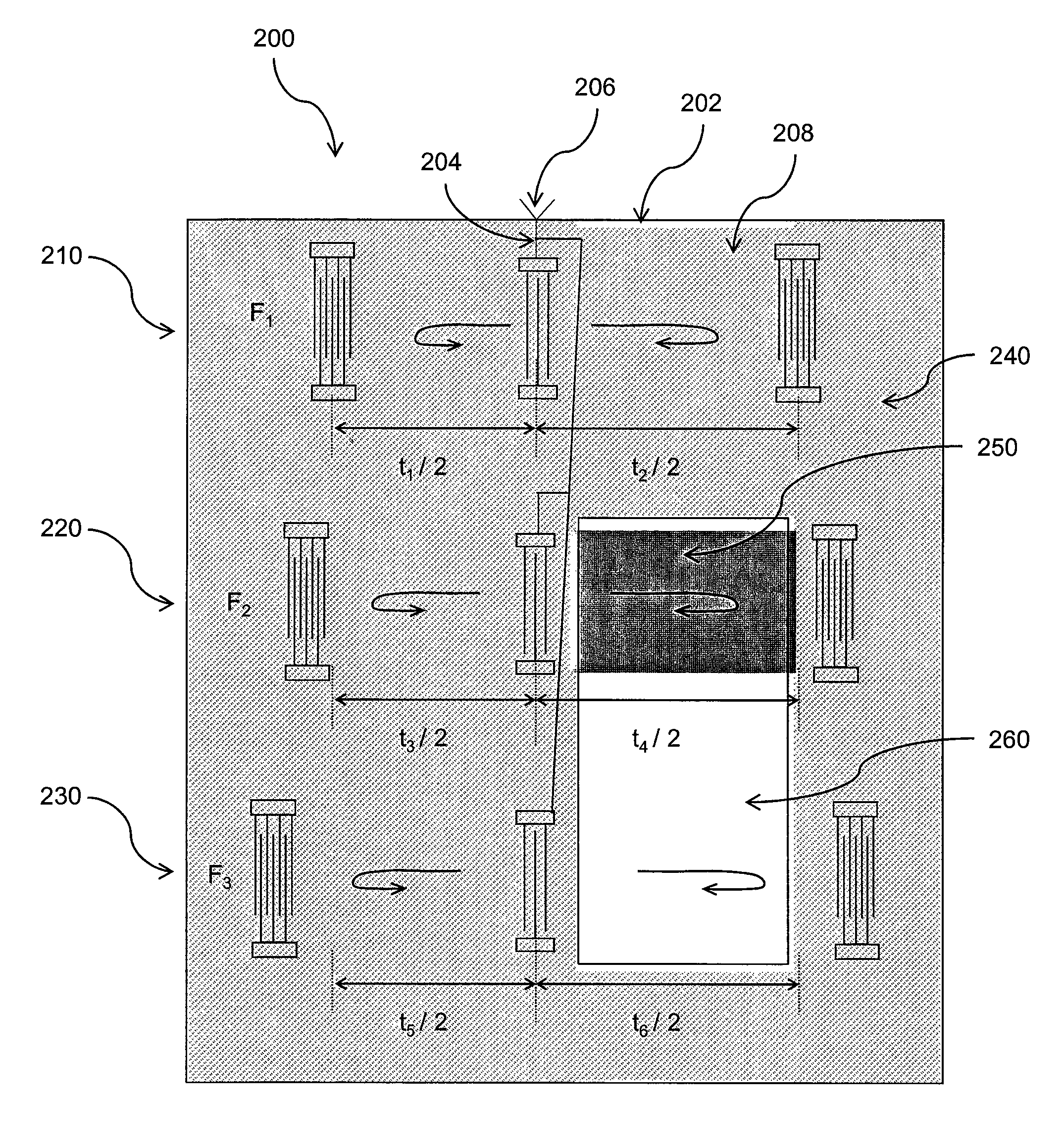
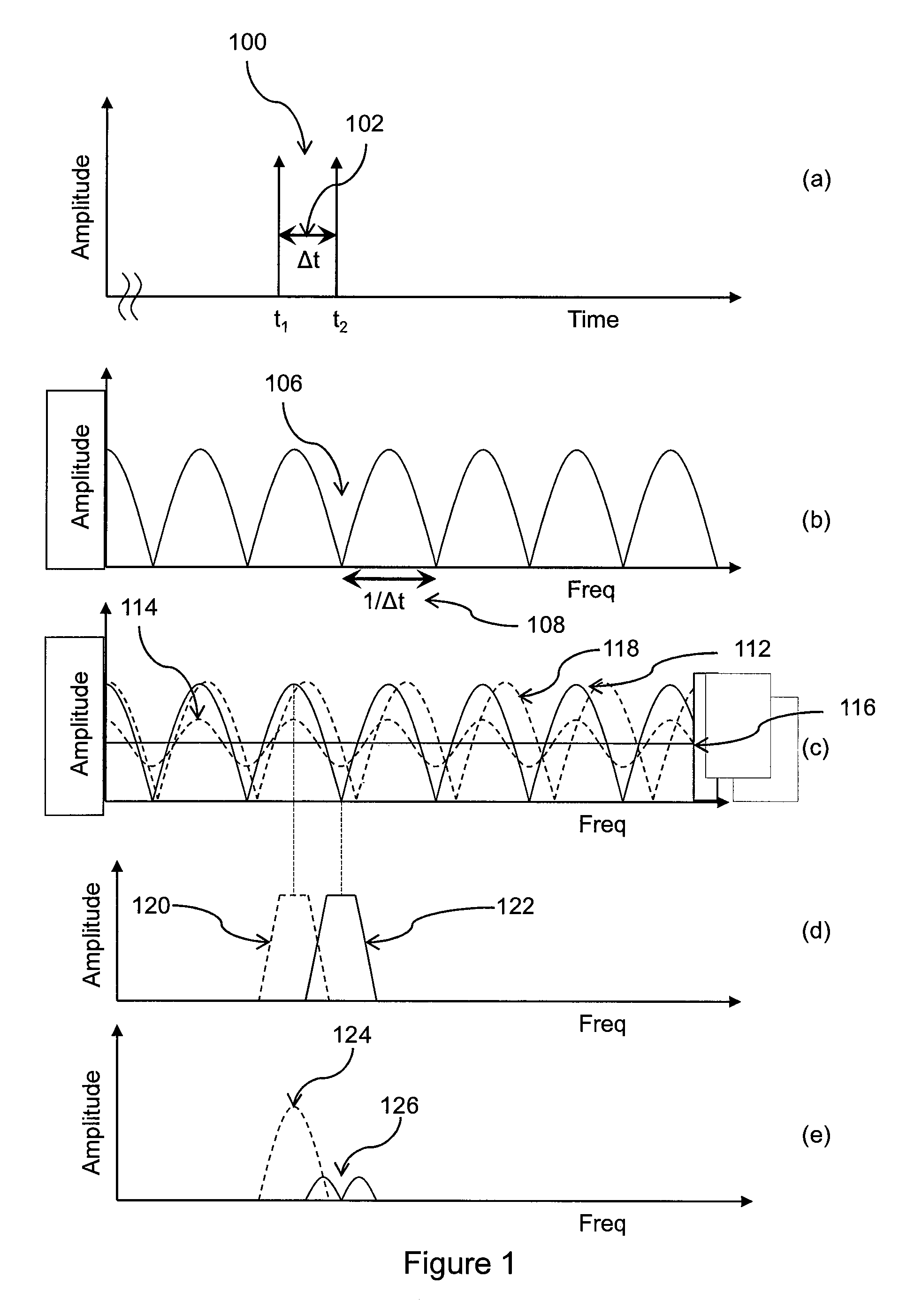
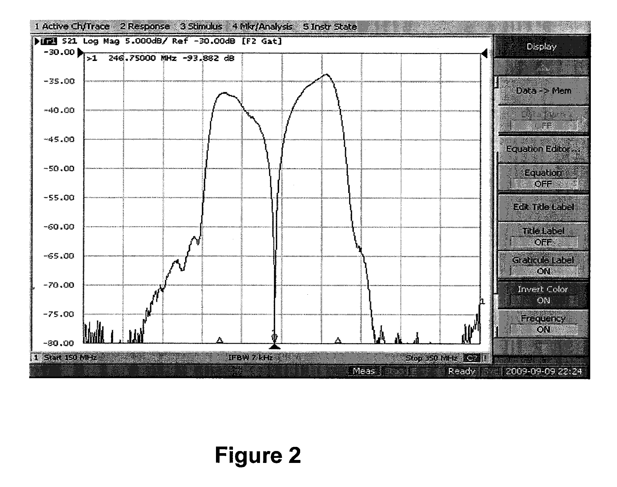
[0046]It has been established (see ASR&D U.S. Pat. No. 7,434,989 SAW temperature sensor and system, issued in 2008, herein incorporated by reference in its entirety) that SAW devices with three acoustic wave elements including at least one transducer can be constructed to produce two responses that are closely spaced in time, resulting in a train of notches in the frequency domain separated by the inverse of the delay difference in responses, windowed by the bandpass function produced by the SAW transducer and reflector elements. FIG. 1 below illustrates idealized versions of the responses described. FIG. 1(a) shows two idealized impulse responses 100 in the time domain, separated by a time spacing Δt (102). FIG. 1(b) shows the (positive) frequency spectrum corresponding to the Fourier transform of the signal in FIG. 1(a), which consists of a train of nulls 106 separated in frequency by spacing 1 / Δt (108). FIG. 1(c) shows how this train of nulls would change as the amplitude of the ...


PUM

PropertyMeasurementUnit
thicknessesaaaaaaaaaa
thickaaaaaaaaaa

Abstract

A surface acoustic wave (SAW) based thin film deposition monitor device and system for monitoring the deposition of ultra-thin films and nanomaterials and the analysis thereof is characterized by acoustic wave device embodiments that include differential delay line device designs, and which can optionally have integral reference devices fabricated on the same substrate as the sensing device, or on a separate device in thermal contact with the film monitoring / analysis device, in order to provide inherently temperature compensated measurements. These deposition monitor and analysis devices can include inherent temperature compensation, higher sensitivity to surface interactions than quartz crystal microbalance (QCM) devices, and the ability to operate at extreme temperatures.

Description

CROSS-REFERENCE TO RELATED APPLICATIONS[0001]This application claims the benefit of U.S. Provisional Application No. 61 / 512,908, filed Jul. 28, 2011, herein incorporated by reference in its entirety.STATEMENT REGARDING FEDERALLY SPONSORED RESEARCH OR DEVELOPMENT[0002]This invention was made with government support under contract NNX10CD41P awarded by the National Aeronautics and Space Administration (NASA). The government has certain rights in the invention.BACKGROUND OF THE INVENTION[0003]1. Field of the Invention[0004]The present invention relates to thin film deposition monitoring and analysis of thin films, and in particular, to apparatus, systems, devices, and methods for monitoring the deposition of ultra-thin films and nanomaterials, and analyzing the properties thereof using surface acoustic wave technology.[0005]2. Description of Related Art[0006]Thin films are deposited by many means, including but not limited to evaporation (thermal or e-beam), sputtering (DC or RF), chem...

Claims


Application Information

Patent Timeline
Patent Type & Authority Patents(United States)
IPC IPC(8): H03H9/25G01N29/12G01N29/24C23C14/54G01N29/036G01N29/02H03H9/205G01H11/08
CPCG01H11/08C23C14/546G01N29/022G01N29/036G01N29/12G01N29/2462H03H9/205G01N2291/0256G01N2291/0422G01N2291/0423
Inventor HINES, JACQUELINE H.
Owner SENSANNA
Why Eureka
Try Eureka