Method for restoring porous surface of dielectric layer by UV light-assisted ALD

a dielectric layer and light-assisted technology, applied in the field of methods, can solve the problems of serious problems, dielectric films, and never been successful in actual industrial applications or on a mass production scale, and achieve the effect of good step coverag

Active Publication Date: 2015-09-15
ASM IP HLDG BV
View PDF7 Cites 380 Cited by
  • Summary
  • Abstract
  • Description
  • Claims
  • Application Information

AI Technical Summary

Benefits of technology

[0008]UV light irradiation as surface treatment in place of plasma exposure can avoid plasma related damage, and can form a thin film with good step coverage. Since process gases for forming a thin film also have the capability to repair low-k damage (damage occurring in dielectric films), the damage repair and thin film formation can be performed at the same time. One of the features of some embodiments is intermittent irradiation of UV light to seal pores and continuously deposit a film on a damaged surface of dielectric film.

Problems solved by technology

However, process-induced damage on dielectric films is related to carbon depletion, moisture absorption, and barrier metal layer diffusion due to their high porosity, and is a very serious problem.
Conventionally, very thin dielectric layers formed by plasma-enhanced chemical vapor deposition (PECVD) or plasma-enhanced atomic layer deposition (PEALD) have been proposed to repair process-induced damage and seal pores at a surface of dielectric films, but they have never been successful on actual industrial applications or on a mass production scale because their step coverage is poor and / or a plasma used in their process also causes damage to surfaces of the dielectric films.

Method used


Image

  • Method for restoring porous surface of dielectric layer by UV light-assisted ALD
  • Method for restoring porous surface of dielectric layer by UV light-assisted ALD
  • Method for restoring porous surface of dielectric layer by UV light-assisted ALD

Examples


example 1

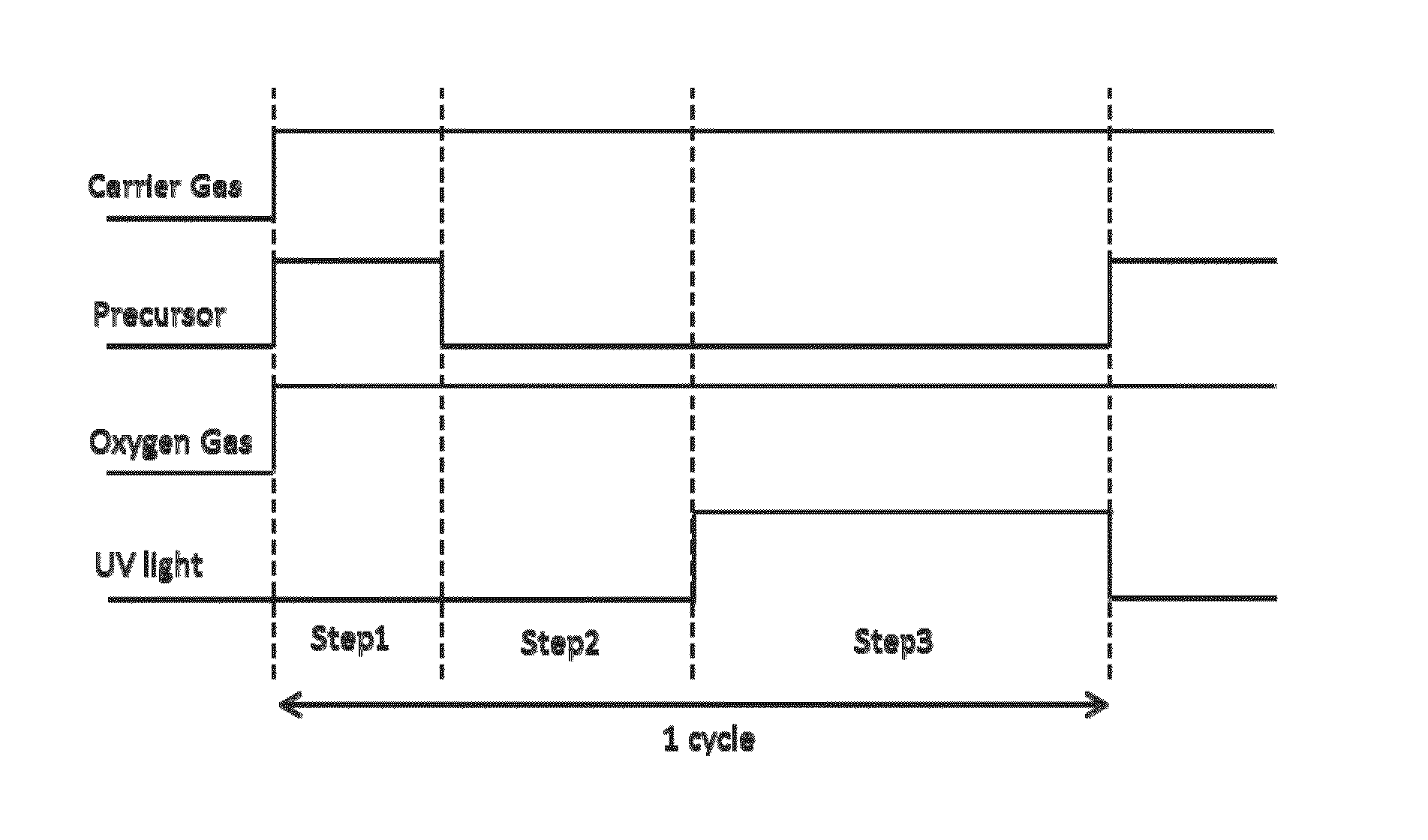
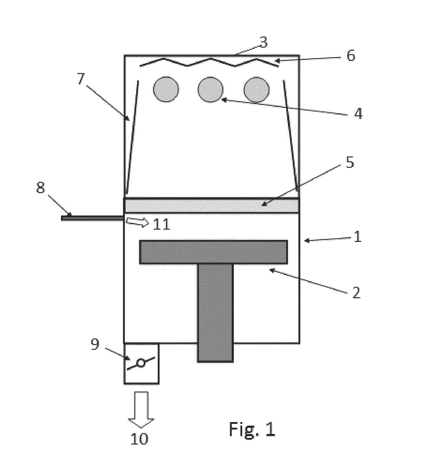
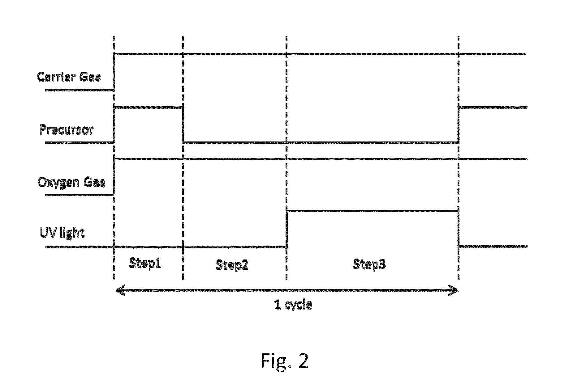
[0057]In this example, the apparatus shown in the schematic diagram of FIG. 1 was used to restore damaged surface of a dielectric film formed on a substrate using the process sequence illustrated in FIG. 2 under the conditions shown in Table 2.

[0058]

TABLE 2Flow rate of precursor gas* (sccm) - intermittent280Duration of supply pulse of precursor gas (seconds) - Step 12.0Type of carrier gasArFlow rate of carrier gas (sccm) - continuous2000Duration of purge (seconds) - Step 25.0Type of oxidizing gasO2Flow rate of oxidizing gas (sccm) - continuous5UV wavelength (nm)365UV power (W / cm2)120Irradiation time (seconds) - Step 310Pressure (Torr)2.0Number of cycles100*Organoaminosilane precursor (BDEAS)

[0059]Method of Experiment

[0060]A Si wafer (300 mm in diameter) on which a porous low-k film (k2.4 siloxane polymer film of 500 nm in film thickness, about 25% in porosity and about 1.2 g / cm3 in density) had been formed via plasma CVD and then exposed to oxygen plasma was transported to the heate...

example 2

[0066]A Si substrate having an isolated pattern (the distance between adjacent convex patterns was so great that the pattern could be considered to be constituted by an isolated pattern) was used and subjected to steps 1 to 4 under the same conditions as in Example 1 to form a repair film on the substrate.

[0067]FIG. 4 is a Scanning Electron Microscope (SEM) photograph of a cross-sectional view of the conformal silicon oxide film formed on the patterned silicon sample (isolated pattern). The step coverage was calculated at 124%.

example 3

[0068]A Si substrate having a dense pattern (the distance between adjacent convex patterns was so close that the pattern could be considered to be constituted by a dense pattern) was used and subjected to steps 1 to 4 under the same conditions as in Example 1 to form a repair film on the substrate.

[0069]FIG. 5 is a Scanning Electron Microscope (SEM) photograph of a cross-sectional view of the conformal silicon oxide film formed on the patterned silicon sample (dense pattern). The step coverage was calculated at 72%.


PUM

PropertyMeasurementUnit
temperatureaaaaaaaaaa
thicknessaaaaaaaaaa
dielectric constantaaaaaaaaaa

Abstract

A method for restoring a porous surface of a dielectric layer formed on a substrate, includes: (i) providing in a reaction space a substrate on which a dielectric layer having a porous surface with terminal hydroxyl groups is formed as an outer layer; (ii) supplying gas of a Si—N compound containing a Si—N bond to the reaction space to chemisorb the Si—N compound onto the surface with the terminal hydroxyl groups; (iii) irradiating the Si—N compound-chemisorbed surface with a pulse of UV light in an oxidizing atmosphere to oxidize the surface and provide terminal hydroxyl groups to the surface; and (iv) repeating steps (ii) through (iii) to form a film on the porous surface of the dielectric layer for restoration.

Description

BACKGROUND OF THE INVENTION[0001]1. Field of the Invention[0002]The present invention generally relates to a method for repairing a damaged surface and / or sealing pores of a surface of a dielectric film.[0003]2. Description of the Related Art[0004]As the size of semiconductor devices has continuously become smaller, a reduction of dielectric constant of dielectric films becomes crucial. However, process-induced damage on dielectric films is related to carbon depletion, moisture absorption, and barrier metal layer diffusion due to their high porosity, and is a very serious problem. Because of the problem, the necessity for technology that repairs the damage and seals the pores of the dielectric films is increasing.[0005]Conventionally, very thin dielectric layers formed by plasma-enhanced chemical vapor deposition (PECVD) or plasma-enhanced atomic layer deposition (PEALD) have been proposed to repair process-induced damage and seal pores at a surface of dielectric films, but they hav...

Claims


Application Information

Patent Timeline
Patent Type & Authority Patents(United States)
IPC IPC(8): H01L21/00H01L21/02H01L21/3105C23C16/34C23C16/455
CPCH01L21/02126C23C16/345C23C16/45536H01L21/0228H01L21/02164H01L21/02222H01L21/02277H01L21/3105
Inventor MATSUSHITA, KIYOHIROARAI, HIROFUMI
Owner ASM IP HLDG BV
Why Eureka
Try Eureka