

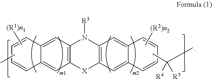
Resist underlayer film-forming composition containing copolymer resin having heterocyclic ring
a copolymer resin and composition technology, applied in the direction of instruments, photomechanical devices, coatings, etc., can solve the problems of difficult to achieve sufficient resist pattern film thickness for substrate fabrication, significant effects, and insufficient resist pattern film thickness, etc., to achieve sufficient etching resistance, excellent resist pattern shape, and efficient suppression of reflection from the substrate
- Summary
- Abstract
- Description
- Claims
- Application Information
AI Technical Summary
Benefits of technology
Problems solved by technology
Method used
Image

Examples
synthesis example 1
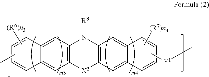
[0122]8.0 g of phenothiazine (manufactured by Tokyo Chemical Industry Co., Ltd.), 6.3 g of 1-naphthaldehyde, (manufactured by Tokyo Chemical Industry Co., Ltd.), 0.81 g of p-toluenesulfonic acid monohydrate (manufactured by Tokyo Chemical Industry Co., Ltd.), and 35.2 g of 1,4-dioxane (manufactured by Kanto Chemical Co., Inc.) were put in a 100-ml recovery flask. Thereafter, the interior of the flask was purged with nitrogen, and then the flask was heated with stirring under reflux for about 28 hours. After the reaction was completed, the solution was diluted with 10 g of 1,4-dioxane (manufactured by Kanto Chemical Co., Inc.). The diluted solution was dropped into a mixed solution of methanol / 28% aqueous ammonia (500 g / 5 g) for reprecipitation. The obtained precipitate was suction-filtered, and the residue was washed with methanol and then dried under reduced pressure for one night at 85° C., whereby 5.8 g of novolak resin was obtained. The obtained polymer corresponded to that of F...
synthesis example 2
[0123]12.0 g of phenothiazine (manufactured by Tokyo Chemical Industry Co., Ltd.), 6.4 g of benzaldehyde (manufactured by Tokyo Chemical Industry Co., Ltd.), 1.2 g of p-toluenesulfonic acid monohydrate (manufactured by Tokyo Chemical Industry Co., Ltd.), and 112.8 g of 1,4-dioxane (manufactured by Kanto Chemical Co., Inc.) were put in a 100-ml recovery flask. Thereafter, the interior of the flask was purged with nitrogen, and then the flask was heated with stirring under reflux for about 26 hours. After the reaction was completed, the solution was diluted with 22 g of tetrahydrofuran (manufactured by Kanto Chemical Co., Inc.). The diluted solution was dropped into 750 g of methanol for reprecipitation. The obtained precipitate was suction-filtered, and the residue was washed with methanol and then dried under reduced pressure for one night at 85° C., whereby 2.2 g of novolak resin was obtained. The obtained polymer corresponded to that of Formula (2-2). The weight-average molecular ...
synthesis example 3
[0124]10.0 g of phenothiazine (manufactured by Tokyo Chemical Industry Co., Ltd.), 9.1 g of 9-fluorenone (manufactured by Tokyo Chemical Industry Co., Ltd.), 1.0 g of p-toluenesulfonic acid monohydrate (manufactured by Tokyo Chemical Industry Co., Ltd.), and 46.8 g of toluene (manufactured by Kanto Chemical Co., Inc.) were put in a 100-ml recovery flask. Thereafter, the interior of the flask was purged with nitrogen, and then the flask was heated with stirring under reflux for about 29 hours. After the reaction was completed, the solution was diluted with 10.4 g of tetrahydrofuran (manufactured by Kanto Chemical Co., Inc.). The diluted solution was dropped into 800 ml of methanol for reprecipitation. The obtained precipitate was suction-filtered, and the residue was washed with methanol and then dried under reduced pressure for one night at 85° C., whereby 12.4 g of novolak resin was obtained. The obtained polymer corresponded to that of Formula (2-3). The weight-average molecular w...
PUM
| Property | Measurement | Unit |
|---|---|---|
| wavelength | aaaaa | aaaaa |
| wavelength | aaaaa | aaaaa |
| wavelength | aaaaa | aaaaa |
Abstract
Description
Claims
Application Information